|
|
|
PDF ACT4523 Data sheet ( Hoja de datos )
| Número de pieza | ACT4523 | |
| Descripción | Wide-Input Sensorless CC/CV Step-Down DC/DC Converter | |
| Fabricantes | Active-Semi | |
| Logotipo | ||
Hay una vista previa y un enlace de descarga de ACT4523 (archivo pdf) en la parte inferior de esta página. Total 15 Páginas | ||
|
No Preview Available !
ACT4523
Rev 7, 01-Aug-13
Wide-Input Sensorless CC/CV Step-Down DC/DC Converter
FEATURES
• 40V Input Voltage Surge
• 38V Steady State Operation
• Up to 3A output current
• Output Voltage up to 12V
• Patent Pending Active CC Sensorless Constant
Current Control
− Integrated Current Control Improves
Efficiency, Lowers Cost, and Reduces
Component Count
• Resistor Programmable
− Current Limit from 1.5A to 3A
− Patented Cable Compensation from 0Ω to
0.3Ω
• ±7.5% CC Accuracy
− Compensation of Input /Output Voltage Change
− Temperature Compensation
− Independent of inductance and Inductor DCR
• 2% Feedback Voltage Accuracy
• Up to 94% Efficiency
• 225kHz Switching Frequency Eases EMI Design
• Advanced Feature Set
− Integrated Soft Start
− Thermal Shutdown
− Secondary Cycle-by-Cycle Current Limit
− Protection Against Shorted ISET Pin
• SOP-8EP Package
APPLICATIONS
• Car Charger/ Adaptor
• Rechargeable Portable Devices
• General-Purpose CC/CV Supply
GENERAL DESCRIPTION
ACT4523 is a wide input voltage, high efficiency
Active CC step-down DC/DC converter that
operates in either CV (Constant Output Voltage)
mode or CC (Constant Output Current) mode.
ACT4523 provides up to 3A output current at
225kHz switching frequency.
Active CC is a patent-pending control scheme to
achieve highest accuracy sensorless constant
current control. Active CC eliminates the expensive,
high accuracy current sense resistor, making it ideal
for battery charging applications and adaptors with
accurate current limit. The ACT4523 achieves
higher efficiency than traditional constant current
switching regulators by eliminating its associated
power loss.
Protection features include cycle-by-cycle current
limit, thermal shutdown, and frequency foldback at
short circuit. The devices are available in a SOP-
8EP package and require very few external devices
for operation.
Input 10V to 40V
ENABLE
HSB
IN SW
ACT4523
EN FB
ISET GND COMP
C3
22nF
50V
L1 30µH
R2 52k
5V
C1
47µF
R1 C2
R4
11.5k 2.2nF
10k
R3
8.2k
D1
SK34
C4
220µF
Innovative PowerTM
-1-
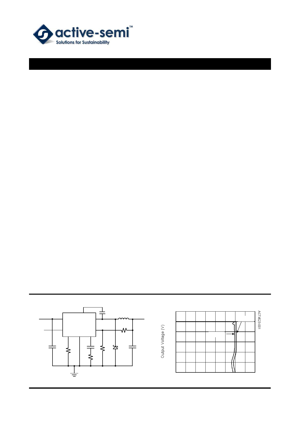
CC/CV Curve
6.0
5.0 VIN = 24V
4.0
VIN = 12V
3.0
2.0
1.0
0.0
0 0.4 0.8 1.2 1.6 2.0 2.4 2.8 3.2
Output Current (A)
www.active-semi.com
Copyright © 2013 Active-Semi, Inc.
1 page 
FUNCTIONAL BLOCK DIAGRAM
AVIN
IN
BANDGAP,
REGULATOR,
EN &
OSCILLATOR
SHUTDOWN
CONTROL
VREF = 0.808V
Σ
PVIN
EMI
CONTROL
PWM
CONTROLLER
VREF = 0.808V
+
FB -
CC
CONTROL
ACT4523
Rev 7, 01-Aug-13
HSB
SW
COMP
ISET
FUNCTIONAL DESCRIPTION
CV/CC Loop Regulation
As seen in Functional Block Diagram, the ACT4523
is a peak current mode pulse width modulation
(PWM) converter with CC and CV control. The
converter operates as follows:
A switching cycle starts when the rising edge of the
Oscillator clock output causes the High-Side Power
Switch to turn on and the Low-Side Power Switch to
turn off. With the SW side of the inductor now
connected to IN, the inductor current ramps up to
store energy in the magnetic field. The inductor
current level is measured by the Current Sense
Amplifier and added to the Oscillator ramp signal. If
the resulting summation is higher than the COMP
voltage, the output of the PWM Comparator goes
high. When this happens or when Oscillator clock
output goes low, the High-Side Power Switch turns
off.
At this point, the SW side of the inductor swings to
a diode voltage below ground, causing the inductor
current to decrease and magnetic energy to be
transferred to output. This state continues until the
cycle starts again. The High-Side Power Switch is
driven by logic using HSB as the positive rail. This
pin is charged to VSW + 5V when the Low-Side
Power Switch turns on. The COMP voltage is the
integration of the error between FB input and the
internal 0.808V reference. If FB is lower than the
reference voltage, COMP tends to go higher to
increase current to the output. Output current will
increase until it reaches the CC limit set by the ISET
resistor. At this point, the device will transition from
regulating output voltage to regulating output
current, and the output voltage will drop with
increasing load.
The Oscillator normally switches at 225kHz.
However, if FB voltage is less than 0.6V, then the
switching frequency decreases until it reaches a
typical value of 30kHz at VFB = 0.15V.
Enable Pin
The ACT4523 has an enable input EN for turning
the IC on or off. The EN pin contains a precision
1.6V comparator with 125mV hysteresis and a 4µA
pull-up current source. The comparator can be used
with a resistor divider from VIN to program a startup
voltage higher than the normal UVLO value. It can
be used with a resistor divider from VOUT to disable
charging of a deeply discharged battery, or it can be
used with a resistor divider containing a thermistor
to provide a temperature-dependent shutoff
protection for over temperature battery. The
thermistor should be thermally coupled to the
battery pack for this usage.
If left floating, the EN pin will be pulled up to roughly
5V by the internal 4µA current source. It can be
driven from standard logic signals greater than
1.6V, or driven with open-drain logic to provide
digital on/off control.
Thermal Shutdown
The ACT4523 disables switching when its junction
temperature exceeds 150°C and resumes when the
temperature has dropped by 20°C.
Innovative PowerTM
- 5 - www.active-semi.com
Copyright © 2013 Active-Semi, Inc.
5 Page 
TYPICAL PERFORMANCE CHARACTERISTICS
(L = 33µH, CIN = 10µF, COUT = 47µF, Ta = 25°C, RCOMP = 8.2k, CCOMP1 = 2.2nF, CCOMP2 = NC)
ACT4523
Rev 7, 01-Aug-13
100
95
90
85
80
75
70
65
60
200
Efficiency vs. Load current
VIN = 12V
VIN = 24V
VOUT = 5V
600
1000
1400 1800
Load Current (mA)
2200
Switching Frequency vs. Feedback Voltage
260
210
160
110
60
10
0 100 200 300 400 500 600 700 800 900
Feedback Voltage (mV)
Switching Frequency vs. Input Voltage
250
230
210
190
170
150
130
110
10 15 20 25 30 35 40
Input Voltage (V)
2700
2600
2500
2400
2300
2200
2100
2000 25
CC Current vs. Temperature
45 65 85 105 125 145
Temperature (°C)
CC Current vs. Input Voltage
2600
2400
2200
2000
1800
1600
10 14 18 22 26 30 34 38
Input Voltage (V)
Maximum Peak Current vs. Duty Cycle
4.2
4.05
3.9
3.75
3.6
3.45
3.3
3.15
3
20
30 40 50
Duty Cycle
60 70
Innovative PowerTM
- 11 -
www.active-semi.com
Copyright © 2013 Active-Semi, Inc.
11 Page | ||
| Páginas | Total 15 Páginas | |
| PDF Descargar | [ Datasheet ACT4523.PDF ] | |
Hoja de datos destacado
| Número de pieza | Descripción | Fabricantes |
| ACT4523 | Wide-Input Sensorless CC/CV Step-Down DC/DC Converter | Active-Semi |
| ACT4523A | Wide-Input Sensorless CC/CV Step-Down DC/DC Converter | Active-Semi |
| ACT4524 | 40V/3.5A Buck Converter | Active-Semi |
| ACT4525 | 40V/3.5A CV/CC Buck Converter | Active-Semi |
| Número de pieza | Descripción | Fabricantes |
| SLA6805M | High Voltage 3 phase Motor Driver IC. |
Sanken |
| SDC1742 | 12- and 14-Bit Hybrid Synchro / Resolver-to-Digital Converters. |
Analog Devices |
|
DataSheet.es es una pagina web que funciona como un repositorio de manuales o hoja de datos de muchos de los productos más populares, |
| DataSheet.es | 2020 | Privacy Policy | Contacto | Buscar |