|
|
PDF GX4002 Data sheet ( Hoja de datos )
| Número de pieza | GX4002 | |
| Descripción | 2x2 14.025Gb/s Crosspoint Switch | |
| Fabricantes | Gennum | |
| Logotipo |  |
|
Hay una vista previa y un enlace de descarga de GX4002 (archivo pdf) en la parte inferior de esta página. Total 30 Páginas | ||
|
No Preview Available !
GX4002 2x2 14.025Gb/s Crosspoint Switch with Trace Equalization and Output
De-Emphasis
Key Features
• 2 x 2 crosspoint switch architecture
• Integrated CDR with 9.95 to 11.3Gb/s and 14.025Gb/s
reference-free operation
• Automatic rate detect
• Dynamic on-chip power management control
• Multiple user-programmable power-down saving
modes
• Independent programmable input trace equalization to
reduce deterministic jitter (ISI)
• Independent programmable output pre-emphasis for
driving long board traces
• Digital control through I2C interface
• Integrated analog-to-digital converter, which provides
access to digital diagnostic information on supply
voltage and die temperature
• Integrated eye monitor and PRBS7 generator/checker
• Polarity invert, output mute functions available
• Single 3.3V supply (±5%)
• On-chip I/O termination
• Low power consumption: 600mW typical
Low power option for 4.25 & 8.5Gb/s operation:
415mW typical
• 5mm x 5mm 32-pin QFN package
• -40°C to +100°C case operation
• RoHS-compliant
Applications
• Enterprise and carrier applications
• 10GbE, Fibre Channel and InfiniBand networks
• Redundancy switching
• Retimer for 10Gb/s and 14Gb/s backplane and
linecards
Description
The GX4002 is a low-power, high-speed 2 x 2 crosspoint
switch, with robust signal conditioning circuits for driving
and receiving high-speed signals through backplanes.
The device consumes as low as 600mW of power (typical)
with all channels operational. Unused portions of the chip
can be turned off in order to further reduce power
consumption.
The signal conditioning features of the GX4002 include
per-input clock and data recovery (CDR), programmable
equalization and per-output programmable de-emphasis.
The input equalizer removes ISI jitter—typically caused by
PCB trace losses—by opening the input data eye in
applications where long PCB traces are used. The
integrated CDR “resets” the jitter budget, effectively
erasing the signal distortion that can occur during
transmission.
Output pre-emphasis capability provides a boost of the
high-frequency content of the output signal, such that the
data eye remains open after passing through a long
interconnect of PCB traces and connectors.
The GX4002 features an integrated analog-to-digital
converter, which, through the serial interface, provides
digital diagnostic information about supply voltage and die
temperature.
The GX4002 device is packaged in a small-outline 5mm ×
5mm 32-pin, high-frequency QFN package with exposed
pad.
The GX4002 is Pb-free, and the encapsulation compound
does not contain halogenated flame retardant. This
component and all homogeneous sub components are
RoHS-compliant.
GX4002 2x2 14.025Gb/s Crosspoint Switch with Trace
Equalization and Output De-Emphasis
Data Sheet
55972 - 0
March 2012
www.gennum.com
1 of 74
Proprietary & Confidential
1 page 
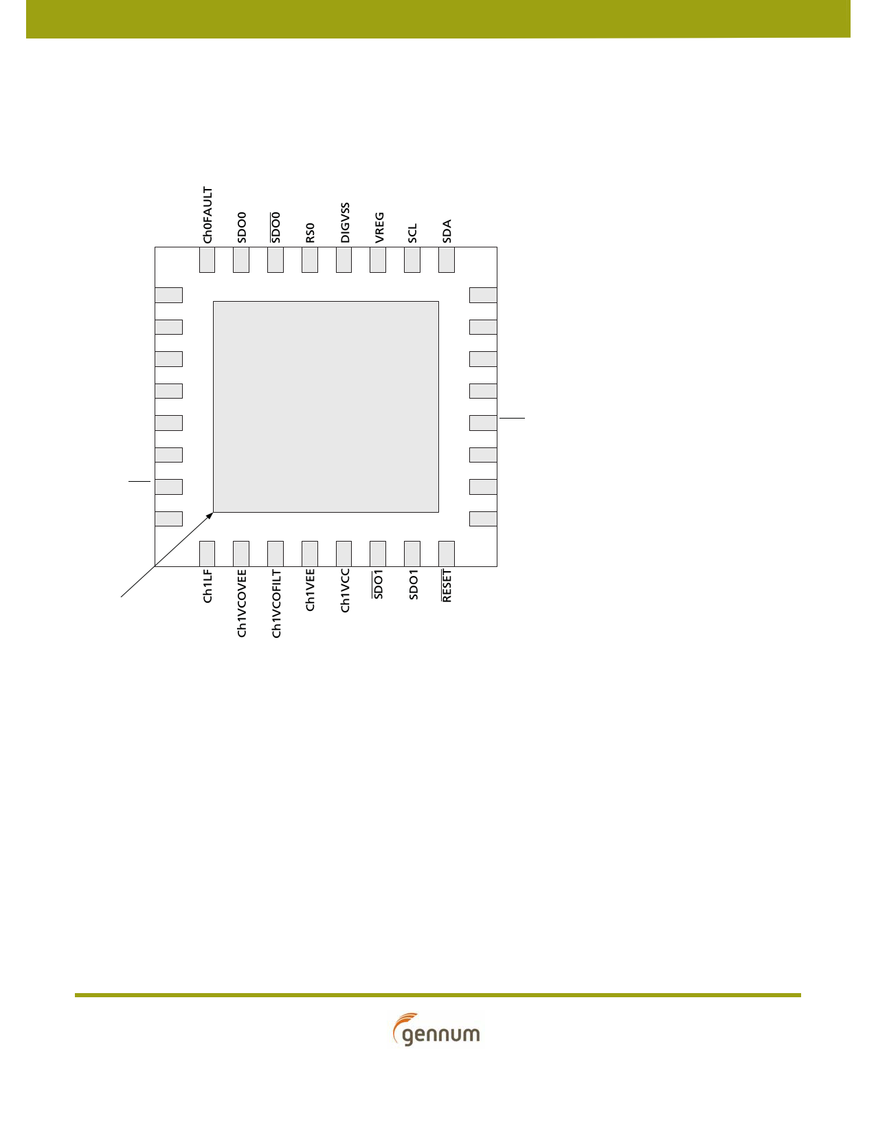
1. Pin Out
1.1 Pin Assignment
SDO0VCC
SDO0VEE
NC
NC
RS1
SDI1
SDI1
Ch1LOS
32 31 30 29 28 27 26 25
1 24
2 23
3 22
4
GX4002
21
32-pin QFN
5
(top view)
20
6 19
7 18
8
9
17
10 11 12 13 14 15 16
GND
Ch0LF
Ch0VCOVEE
Ch0VCOFILT
SDI0
SDI0
Ch0VEE
Ch0VCC
Ground Pad
(bottom of package)
Figure 1-1: GX4002 Pin Assignment
GX4002 2x2 14.025Gb/s Crosspoint Switch with Trace
Equalization and Output De-Emphasis
Data Sheet
55972 - 0
March 2012
5 of 74
Proprietary & Confidential
5 Page 
Table 2-3: AC Electrical Characteristics (Continued)
VCC = +2.8V to +3.47V, TC = -40°C to 100°C. Typical values are VCC = +3.3V and TA = 25°C, unless otherwise specified.
Specifications assume default setting to end-terminated 50Ω transmission lines, unless otherwise stated. Typical Data Rate = 14.025Gb/s
Parameter
Conditions
Symbol
Min
Typ
Max
Units Notes
1 sigma, IC to IC
—
1.50
—
mVrms
—
Ch1LOS Threshold Level
Variation
over VCC Range
over temperature
range -40°C to
+100°C
— +0.5 — dB —
— +0.5 — dB —
Ch1LOS Threshold Level
Hysteresis Setting Range
electrical
0 — 6 dB —
Ch1LOS Response Time
3 5 20 μs —
Ch1 CDR Lock Time
16G FC mode: loop
filter cap = 100nF
— — 0.5 ms 4
Differential Output Voltage
Setting Range
minimum swing
setting
maximum swing
setting
—
100
—
mVppd
—
—
850
—
mVppd
—
Output Pre-emphasis
Setting Range
maximum setting
3 — — dB 5
NOTES:
1. See Table 3-1 for details.
2. At 7GHz.
3. 600mVppd swing.
4. For loop bandwidth = 13MHz (as detailed in Table 3-4).
5. 600mVppd swing.
6. At 7GHz (dielectric loss).
7. Reg89[7:0] = "11001000" = Reg110[7:0]. Reg90[1:0] = "00" = Reg111[7:0]. Reg102[1:0] = "00". Reg118[4:3] = "11" = Reg119[4:3].
Reg80[7:0] = "11101110". Reg81[4:0] = "11100" = Reg103[4:0]. Reg82[4:0] = "11010" = Reg104[4:0].
8. Reg89[7:0] = "11111111" = Reg110[7:0]. Reg90[1:0] = "11" = Reg111[7:0]. Reg102[1:0] = "00". Reg118[4:3] = "00" = Reg119[4:3].
Reg80[7:0] = "01000100". Reg81[4:0] = "01000" = Reg103[4:0]. Reg82[4:0] = "10000" = Reg104[4:0].
GX4002 2x2 14.025Gb/s Crosspoint Switch with Trace
Equalization and Output De-Emphasis
Data Sheet
55972 - 0
March 2012
11 of 74
Proprietary & Confidential
11 Page | ||
| Páginas | Total 30 Páginas | |
| PDF Descargar | [ Datasheet GX4002.PDF ] | |
Hoja de datos destacado
| Número de pieza | Descripción | Fabricantes |
| GX4002 | 2x2 14.025Gb/s Crosspoint Switch | Gennum |
| Número de pieza | Descripción | Fabricantes |
| SLA6805M | High Voltage 3 phase Motor Driver IC. |
Sanken |
| SDC1742 | 12- and 14-Bit Hybrid Synchro / Resolver-to-Digital Converters. |
Analog Devices |
|
DataSheet.es es una pagina web que funciona como un repositorio de manuales o hoja de datos de muchos de los productos más populares, |
| DataSheet.es | 2020 | Privacy Policy | Contacto | Buscar |
