|
|
PDF 3804 Data sheet ( Hoja de datos )
| Número de pieza | 3804 | |
| Descripción | SINGLE-CHIP 8-BIT CMOS MICROCOMPUTER | |
| Fabricantes | Renesas | |
| Logotipo |  |
|
Hay una vista previa y un enlace de descarga de 3804 (archivo pdf) en la parte inferior de esta página. Total 30 Páginas | ||
|
No Preview Available !
3803/3804 Group
SINGLE-CHIP 8-BIT CMOS MICROCOMPUTER
REJ03B0073-0401Z
Rev.4.01
Nov 14, 2003
DESCRIPTION
The 3803/3804 group is the 8-bit microcomputer based on the 740
family core technology.
The 3803/3804 group is designed for household products, office
automation equipment, and controlling systems that require ana-
log signal processing, including the A-D converter and D-A
converters.
The 3804 group is the version of the 3803 group to which an I2C-
BUS control function has been added.
FEATURES
qBasic machine-language instructions ...................................... 71
qMinimum instruction execution time ................................ 0.24 µs
(at 16.8 MHz oscillation frequency)
qMemory size
ROM ............................................................... 16 K to 60 K bytes
RAM ................................................................. 640 to 2048 bytes
qProgrammable input/output ports ............................................ 56
qSoftware pull-up resistors ................................................. Built-in
q Interrupts
21 sources, 16 vectors ............................................... 3803 group
(external 8, internal 12, software 1)
23 sources, 16 vectors ............................................... 3804 group
(external 9, internal 13, software 1)
qTimers ........................................................................... 16-bit ✕ 1
8-bit ✕ 4
(with 8-bit prescaler)
qWatchdog timer ............................................................ 16-bit ✕ 1
qSerial I/O ...................... 8-bit ✕ 2 (UART or Clock-synchronized)
8-bit ✕ 1 (Clock-synchronized)
qPWM ............................................ 8-bit ✕ 1 (with 8-bit prescaler)
qI2C-BUS interface (3804 group only) ........................... 1 channel
qA-D converter ............................................. 10-bit ✕ 16 channels
(8-bit reading enabled)
qD-A converter ................................................. 8-bit ✕ 2 channels
qLED direct drive port .................................................................. 8
qClock generating circuit ..................................... Built-in 2 circuits
(connect to external ceramic resonator or quartz-crystal oscillator)
qPower source voltage
In high-, middle-speed mode
At 16.8 MHz oscillation frequency ............................ 4.5 to 5.5 V
At 12.5 MHz oscillation frequency ............................ 4.0 to 5.5 V
At 8.38 MHz oscillation frequency) ........................ 2.7 to 5.5 V ✽
In low-speed mode
At 32 kHz oscillation frequency .............................. 2.7 to 5.5 V ✽
(✽ This value of flash memory version is 4.0 to 5.5 V.)
qPower dissipation
In high-speed mode ................................................ 60 mW (typ.)
(at 16.8 MHz oscillation frequency, at 5 V power source voltage)
In low-speed mode ................................................... 60 µW (typ.)
(at 32 kHz oscillation frequency, at 3 V power source voltage)
qOperating temperature range .................................... –20 to 85°C
q Packages
SP .................................................. 64P4B (64-pin 750 mil SDIP)
FP ....................................... 64P6N-A (64-pin 14 ✕ 14 mm QFP)
HP ..................................... 64P6Q-A (64-pin 10 ✕ 10 mm LQFP)
<Flash memory mode>
qSupply voltage ................................................. VCC = 5 V ± 10 %
qProgram/Erase voltage ........................... VPP = 11.7 V to 12.6 V
qProgramming method ...................... Programming in unit of byte
qErasing method
Batch erasing ........................................ Parallel/Serial I/O mode
Block erasing .................................... CPU reprogramming mode
qProgram/Erase control by software command
qNumber of times for programming/erasing ............................ 100
q Operating temperature range (at programming/erasing) ...........
........................................................................ Room temperature
sNotes
1. The flash memory version cannot be used for application em-
bedded in the MCU card.
2. Supply voltage Vcc of the flash memory version is 4.0 to 5.5
V.
Rev.4.01 Nov 14, 2003 page 1 of 136
1 page 
3803/3804 Group
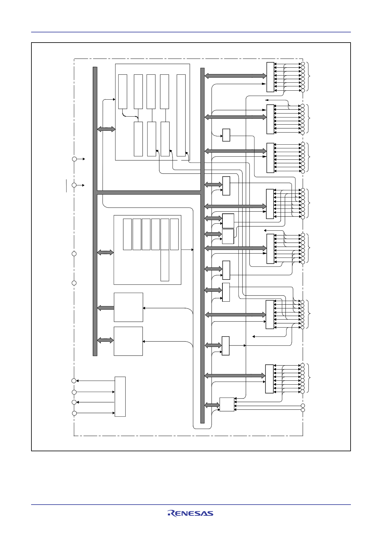
Fig. 6 3804 group functional block diagram
Rev.4.01 Nov 14, 2003 page 5 of 136
5 Page 
3803/3804 Group
FUNCTIONAL DESCRIPTION
CENTRAL PROCESSING UNIT (CPU)
The 3803/3804 group uses the standard 740 Family instruction
set. Refer to the table of 740 Family addressing modes and ma-
chine instructions or the 740 Family Software Manual for details
on the instruction set.
Machine-resident 740 Family instructions are as follows:
The FST and SLW instructions cannot be used.
The STP, WIT, MUL, and DIV instructions can be used.
[Accumulator (A)]
The accumulator is an 8-bit register. Data operations such as data
transfer, etc., are executed mainly through the accumulator.
[Index Register X (X)]
The index register X is an 8-bit register. In the index addressing
modes, the value of the OPERAND is added to the contents of
register X and specifies the real address.
[Index Register Y (Y)]
The index register Y is an 8-bit register. In partial instruction, the
value of the OPERAND is added to the contents of register Y and
specifies the real address.
[Stack Pointer (S)]
The stack pointer is an 8-bit register used during subroutine calls
and interrupts. This register indicates start address of stored area
(stack) for storing registers during subroutine calls and interrupts.
The low-order 8 bits of the stack address are determined by the
contents of the stack pointer. The high-order 8 bits of the stack ad-
dress are determined by the stack page selection bit. If the stack
page selection bit is “0” , the high-order 8 bits becomes “0016”. If
the stack page selection bit is “1”, the high-order 8 bits becomes
“0116”.
The operations of pushing register contents onto the stack and
popping them from the stack are shown in Figure 10.
Store registers other than those described in Figure 10 with pro-
gram when the user needs them during interrupts or subroutine
calls.
[Program Counter (PC)]
The program counter is a 16-bit counter consisting of two 8-bit
registers PCH and PCL. It is used to indicate the address of the
next instruction to be executed.
b15
PCH
b7 b0
A Accumulator
b7 b0
X Index register X
b7 b0
Y Index register Y
b7 b0
S Stack pointer
b7 b0
PCL Program counter
b7 b0
N V T B D I Z C Processor status register (PS)
Carry flag
Zero flag
Interrupt disable flag
Decimal mode flag
Break flag
Index X mode flag
Overflow flag
Negative flag
Fig.9 740 Family CPU register structure
Rev.4.01 Nov 14, 2003 page 11 of 136
11 Page | ||
| Páginas | Total 30 Páginas | |
| PDF Descargar | [ Datasheet 3804.PDF ] | |
Hoja de datos destacado
| Número de pieza | Descripción | Fabricantes |
| 380-10-116-00-001 | PCB Header Strips Single row / double row Wire-wrap / solder tail | Precid-Dip Durtal SA |
| 380-90-116-00-001 | PCB Header Strips Single row / double row Wire-wrap / solder tail | Precid-Dip Durtal SA |
| 3803 | SINGLE-CHIP 8-BIT CMOS MICROCOMPUTER | Renesas |
| 3804 | SINGLE-CHIP 8-BIT CMOS MICROCOMPUTER | Renesas |
| Número de pieza | Descripción | Fabricantes |
| SLA6805M | High Voltage 3 phase Motor Driver IC. |
Sanken |
| SDC1742 | 12- and 14-Bit Hybrid Synchro / Resolver-to-Digital Converters. |
Analog Devices |
|
DataSheet.es es una pagina web que funciona como un repositorio de manuales o hoja de datos de muchos de los productos más populares, |
| DataSheet.es | 2020 | Privacy Policy | Contacto | Buscar |
