|
|
|
PDF P4C107 Data sheet ( Hoja de datos )
| Número de pieza | P4C107 | |
| Descripción | STATIC CMOS RAM | |
| Fabricantes | PYRAMID | |
| Logotipo | ||
Hay una vista previa y un enlace de descarga de P4C107 (archivo pdf) en la parte inferior de esta página. Total 8 Páginas | ||
|
No Preview Available !
FEATURES
Full CMOS
High Speed (Equal Access and Cycle Times)
– 10/12/15 ns (Commercial)
– 12/15/20 ns (Industrial)
Single 5V±10% Power Supply
P4C107
ULTRA HIGH SPEED 1M x 1
STATIC CMOS RAM
Separate Data I/O
Three-State Output
Fully TTL Compatible Inputs and Outputs
Standard Pinout (JEDEC Approved)
– 28-Pin 400 mil SOJ
DESCRIPTION
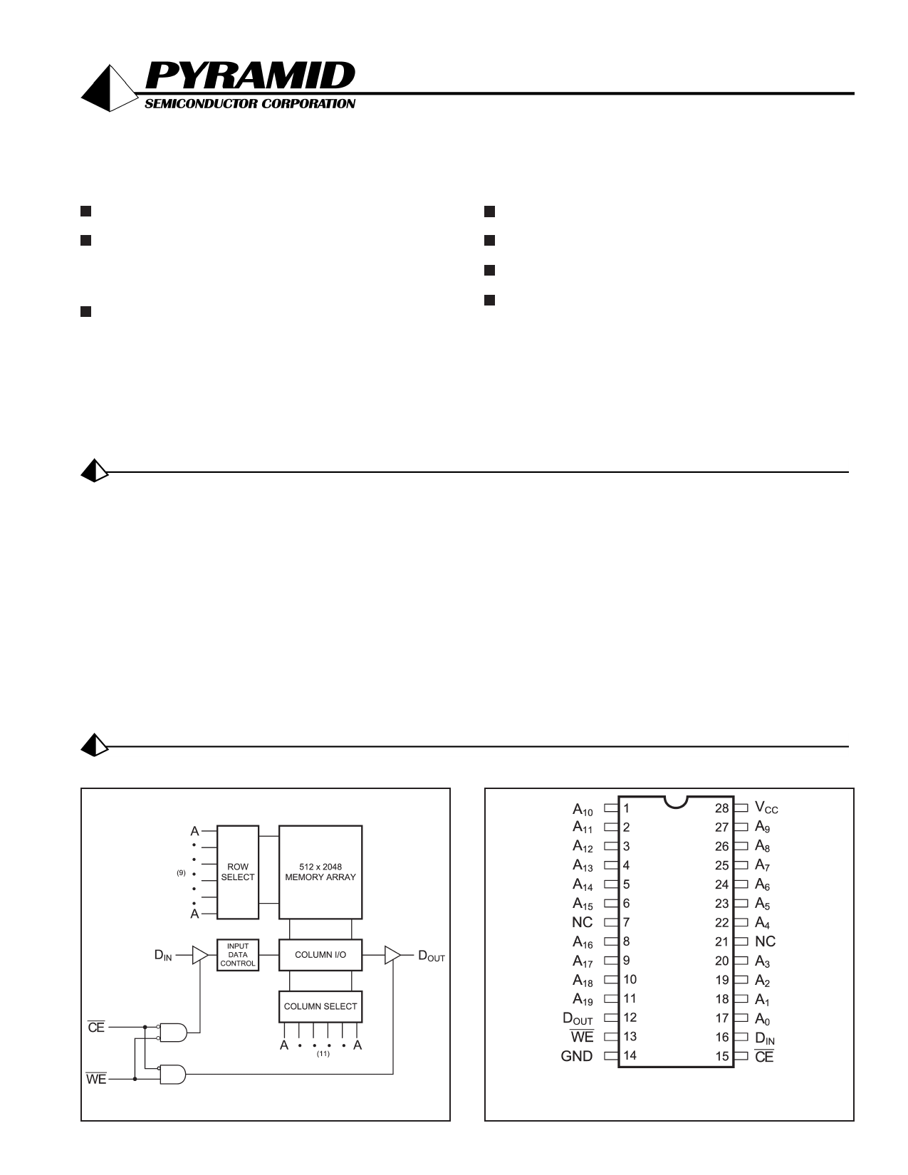
The P4C107 is a 1Mx1-bit ultra high-speed static RAM.
The CMOS memories require no clocks or refreshing and
have equal access and cycle times. The RAM operates
from a single 5V ± 10% tolerance power supply. Data
integrity is maintained for supply voltages down to 2.0V,
typically drawing 50µA.
Access times as fast as 10 nanoseconds are available,
greatly enhancing system speeds.
The P4C107 is available in a 28-pin 400 mil SOJ.
Functional Block Diagram
Pin Configuration
Document # SRAM139 REV OR
SOJ (J7)
Revised April 2010
1 page 
P4C107 - ULTRA HIGH SPEED 1M X 1 STATIC CMOS RAM
Timing Waveform of Write Cycle No. 2 (CE Controlled)(10)
AC TEST CONDITIONS
Input Pulse Levels
Input Rise and Fall Times
Input Timing Reference Level
Output Timing Reference Level
Output Load
GND to 3.0V
3ns
1.5V
1.5V
See Figures 1 and 2
TRUTH TABLE
Mode
CE
Standby
H
Read
L
Write
L
WE
X
H
L
I/O
High Z
DOUT
High Z
Power
Standby
Active
Active
Figure 1. Output Load
* including scope and test fixture.
Note:
Because of the ultra-high speed of the P4C107, care must be taken when
testing this device; an inadequate setup can cause a normal function-
ing part to be rejected as faulty. Long high-inductance leads that cause
supply bounce must be avoided by bringing the VCC and ground planes
directly up to the contactor fingers. A 0.01 µF high frequency capacitor
Figure 2. Thevenin Equivalent
is also required between VCC and ground. To avoid signal reflections,
proper termination must be used; for example, a 50Ω test environment
should be terminated into a 50Ω load with 1.73V (Thevenin Voltage) at
the comparator input, and a 116Ω resistor must be used in series with
DOUT to match 166Ω (Thevenin Resistance).
Notes:
10. CE and WE must be LOW for WRITE cycle.
11. OE is LOW for this WRITE cycle to show tWZ and tOW.
12. If CE goes HIGH simultaneously with WE HIGH, the output remains
in a high impedance state
13. Write Cycle Time is measured from the last valid address to the first
transitioning address.
Document # SRAM139 REV OR
Page 5
5 Page | ||
| Páginas | Total 8 Páginas | |
| PDF Descargar | [ Datasheet P4C107.PDF ] | |
Hoja de datos destacado
| Número de pieza | Descripción | Fabricantes |
| P4C1023 | LOW POWER 128K x 8 SINGLE CHIP ENABLE CMOS STATIC RAM | Pyramid Semiconductor |
| P4C1023L | LOW POWER 128K x 8 SINGLE CHIP ENABLE CMOS STATIC RAM | Pyramid Semiconductor |
| P4C1024 | HIGH SPEED 128K X 8 CMOS STATIC RAM | ETC |
| P4C1024-15J3C | HIGH SPEED 128K X 8 CMOS STATIC RAM | ETC |
| Número de pieza | Descripción | Fabricantes |
| SLA6805M | High Voltage 3 phase Motor Driver IC. |
Sanken |
| SDC1742 | 12- and 14-Bit Hybrid Synchro / Resolver-to-Digital Converters. |
Analog Devices |
|
DataSheet.es es una pagina web que funciona como un repositorio de manuales o hoja de datos de muchos de los productos más populares, |
| DataSheet.es | 2020 | Privacy Policy | Contacto | Buscar |