|
|
|
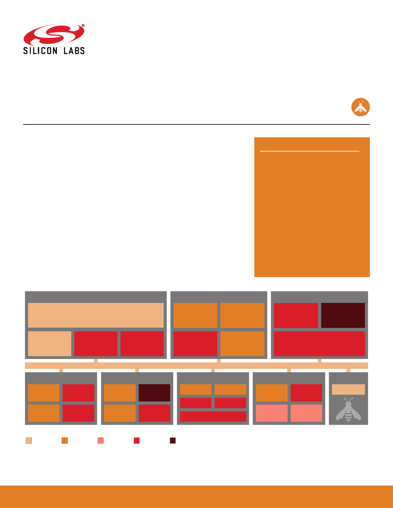
PDF EFM8LB1 Data sheet ( Hoja de datos )
| Número de pieza | EFM8LB1 | |
| Descripción | microcontrollers | |
| Fabricantes | Silicon Laboratories | |
| Logotipo | ||
Hay una vista previa y un enlace de descarga de EFM8LB1 (archivo pdf) en la parte inferior de esta página. Total 30 Páginas | ||
|
No Preview Available !
EFM8 Laser Bee Family
EFM8LB1 Data Sheet
The EFM8LB1, part of the Laser Bee family of MCUs, is a per-
formance line of 8-bit microcontrollers with a comprehensive ana-
log and digital feature set in small packages.
These devices offer state-of-the-art performance by integrating 14-bit ADC, internal
calibrated temperature sensor (±3 °C), and up to four 12-bit DACs into small packages,
making them ideal for the most stringent analog requirement applications. With an effi-
cient, pipelined 8051 core with maximum operating frequency at 72 MHz, various com-
munication interfaces, and four channels of configurable logic, the EFM8LB1 family is
optimal for many embedded applications.
EFM8LB1 applications include the following:
• Optical network modules
• Precision instrumentation
• Industrial control and automation
• Smart sensors
KEY FEATURES
• Pipelined 8-bit 8051 MCU Core with
72 MHz operating frequency
• Up to 29 multifunction I/O pins
• One 14-bit, 900 ksps ADC
• Up to four 12-bit DACs with
synchronization and PWM capabilities
• Two low-current analog comparators with
built-in reference DACs
• Internal calibrated temperature sensor
(±3 °C)
• Internal 72 MHz and 24.5 MHz oscillators
accurate to ±2%
• Four channels of Configurable Logic
• 6-channel PWM / PCA
• Six 16-bit general-purpose timers
Core / Memory
CIP-51 8051 Core
(72 MHz)
Clock Management
External
Oscillator
High Frequency
72 MHz RC
Oscillator
Energy Management
Internal LDO
Regulator
Power-On Reset
Flash Program
Memory
(up to 64 KB)
RAM Memory
(up to 4352 bytes)
Debug Interface
with C2
Low Frequency
RC Oscillator
High Frequency
24.5 MHz RC
Oscillator
Brown-Out Detector
Serial Interfaces
2 x UART
SPI
I2C / SMBus
High-Speed
I2C Slave
I/O Ports
External
Interrupts
Pin Reset
General
Purpose I/O
Pin Wakeup
8-bit SFR bus
Timers and Triggers
Timers
0/1/2/5
Watchdog
Timer
PCA/PWM
Timer 3/4
4 x Configurable Logic Units
Lowest power mode with peripheral operational:
Normal
Idle
Suspend
Snooze
Shutdown
Analog Interfaces
ADC
2x
Comparators
Up to 4 x
Voltage DAC
Internal
Voltage
Reference
Security
16-bit CRC
silabs.com | Smart. Connected. Energy-friendly.
This information applies to a product under development. Its characteristics and specifications are subject to change without notice.
Preliminary Rev. 0.4
1 page 
3. System Overview
3.1 Introduction
EFM8LB1 Data Sheet
System Overview
C2CK/RSTb
C2D
Debug /
Programming
Hardware
Reset
Power-On
Reset
Supply
Monitor
CIP-51 8051 Controller
Core
64 KB ISP Flash
Program Memory
256 Byte SRAM
4096 Byte XRAM
VDD
VREGIN
GND
Power
Net
Voltage
Regulator
Independent
Watchdog
Timer
EXTCLK
XTAL1
XTAL2
System Clock
Configuration
Low Freq.
Oscillator
CMOS Clock
Input
External Crystal /
RC Oscillator
72 MHz 2%
Oscillator
24.5 MHz 2%
Oscillator
SYSCLK
SFR
Bus
Port I/O Configuration
Digital Peripherals
UART0
UART1
Timers 0,
1, 2, 3, 4, 5
6-ch PCA
I2C Slave
Priority
Crossbar
Decoder
I2C /
SMBus
SPI
CRC
Config.
Logic
Units (4)
Crossbar
Control
Analog Peripherals
Internal
Reference
4 12-bit
DACs
VDD
VREF
14/12/10-
bit ADC
VDD
Temp
Sensor
+-+-
2 Comparators
Port 0
Drivers
Port 1
Drivers
Port 2
Drivers
Port 3
Drivers
Figure 3.1. Detailed EFM8LB1 Block Diagram
VIO
P0.n
P1.n
P2.n
P3.n
silabs.com | Smart. Connected. Energy-friendly.
Preliminary Rev. 0.4 | 4
5 Page 
3.7 Analog
EFM8LB1 Data Sheet
System Overview
14/12/10-Bit Analog-to-Digital Converter (ADC0)
The ADC is a successive-approximation-register (SAR) ADC with 14-, 12-, and 10-bit modes, integrated track-and hold and a program-
mable window detector. The ADC is fully configurable under software control via several registers. The ADC may be configured to
measure different signals using the analog multiplexer. The voltage reference for the ADC is selectable between internal and external
reference sources.
• Up to 20 external inputs
• Single-ended 14-bit, 12-bit and 10-bit modes
• Supports an output update rate of up to 1 Msps in 12-bit mode
• Channel sequencer logic with direct-to-XDATA output transfers
• Operation in a low power mode at lower conversion speeds
• Asynchronous hardware conversion trigger, selectable between software, external I/O and internal timer and configurable logic sour-
ces
• Output data window comparator allows automatic range checking
• Support for output data accumulation
• Conversion complete and window compare interrupts supported
• Flexible output data formatting
• Includes a fully-internal fast-settling 1.65 V reference and an on-chip precision 2.4 / 1.2 V reference, with support for using the sup-
ply as the reference, an external reference and signal ground
• Integrated factory-calibrated temperature sensor
12-Bit Digital-to-Analog Converters (DAC0, DAC1, DAC2, DAC3)
The DAC modules are 12-bit Digital-to-Analog Converters with the capability to synchronize multiple outputs together. The DACs are
fully configurable under software control. The voltage reference for the DACs is selectable between internal and external reference
sources.
• Voltage output with 12-bit performance
• Hardware conversion trigger, selectable between software, external I/O and internal timer and configurable logic sources
• Outputs may be configured to persist through reset and maintain output state to avoid system disruption
• Multiple DAC outputs can be synchronized together
• DAC pairs (DAC0 and 1 or DAC2 and 3) support complementary output waveform generation
• Outputs may be switched between two levels according to state of configurable logic / PWM input trigger
• Flexible input data formatting
• Supports references from internal supply, on-chip precision reference, or external VREF pin
Low Current Comparators (CMP0, CMP1)
An analog comparator is used to compare the voltage of two analog inputs, with a digital output indicating which input voltage is higher.
External input connections to device I/O pins and internal connections are available through separate multiplexers on the positive and
negative inputs. Hysteresis, response time, and current consumption may be programmed to suit the specific needs of the application.
The comparator includes the following features:
• Up to 10 (CMP0) or 9 (CMP1) external positive inputs
• Up to 10 (CMP0) or 9 (CMP1) external negative inputs
• Additional input options:
• Internal connection to LDO output
• Direct connection to GND
• Direct connection to VDD
• Dedicated 6-bit reference DAC
• Synchronous and asynchronous outputs can be routed to pins via crossbar
• Programmable hysteresis between 0 and ±20 mV
• Programmable response time
• Interrupts generated on rising, falling, or both edges
• PWM output kill feature
silabs.com | Smart. Connected. Energy-friendly.
Preliminary Rev. 0.4 | 10
11 Page | ||
| Páginas | Total 30 Páginas | |
| PDF Descargar | [ Datasheet EFM8LB1.PDF ] | |
Hoja de datos destacado
| Número de pieza | Descripción | Fabricantes |
| EFM8LB1 | microcontrollers | Silicon Laboratories |
| Número de pieza | Descripción | Fabricantes |
| SLA6805M | High Voltage 3 phase Motor Driver IC. |
Sanken |
| SDC1742 | 12- and 14-Bit Hybrid Synchro / Resolver-to-Digital Converters. |
Analog Devices |
|
DataSheet.es es una pagina web que funciona como un repositorio de manuales o hoja de datos de muchos de los productos más populares, |
| DataSheet.es | 2020 | Privacy Policy | Contacto | Buscar |