|
|
|
PDF AD7768 Data sheet ( Hoja de datos )
| Número de pieza | AD7768 | |
| Descripción | Simultaneous Sampling ADC | |
| Fabricantes | Analog Devices | |
| Logotipo | ||
Hay una vista previa y un enlace de descarga de AD7768 (archivo pdf) en la parte inferior de esta página. Total 30 Páginas | ||
|
No Preview Available !
Data Sheet
8-/4-Channel, 24-Bit, Simultaneous Sampling
ADCs with Power Scaling, 110.8 kHz BW
AD7768/AD7768-4
FEATURES
Precision ac and dc performance
8-/4-channel simultaneous sampling
256 kSPS maximum ADC output data rate per channel
108 dB dynamic range
110.8 kHz maximum input bandwidth (−3 dB bandwidth)
−120 dB total harmonic distortion (THD) typical
±2 ppm of full-scale range (FSR) integral nonlinearity
(INL), ±50 µV offset error, ±30 ppm gain error
Optimized power dissipation vs. noise vs. input bandwidth
Selectable power, speed, and input bandwidth (BW) modes
Fast: highest speed; 110.8 kHz BW, 51.5 mW per channel
Median: half speed, 55.4 kHz BW, 27.5 mW per channel
Eco: lowest power, 13.8 kHz BW, 9.375 mW per channel
Input BW range: dc to 110.8 kHz
Programmable input bandwidth/sampling rates
Cyclic redundancy check (CRC) error checking on data interface
Daisy-chaining
Linear phase digital filter
Low latency sinc5 filter
Wideband brick wall filter: ±0.005 dB pass-band ripple
from dc to 102.4 kHz
Analog input precharge buffers
Power supply
AVDD1 = 5.0 V, AVDD2 = 2.25 V to 5.0 V
IOVDD = 2.5 V to 3.3 V or IOVDD = 1.8 V
64-lead LQFP package, no exposed pad
Temperature range: −40°C to +105°C
APPLICATIONS
Data acquisition systems: USB/PXI/Ethernet
Instrumentation and industrial control loops
Audio test and measurement
Vibration and asset condition monitoring
3-phase power quality analysis
Sonar
High precision medical electroencephalogram (EEG)/
electromyography (EMG)/electrocardiogram (ECG)
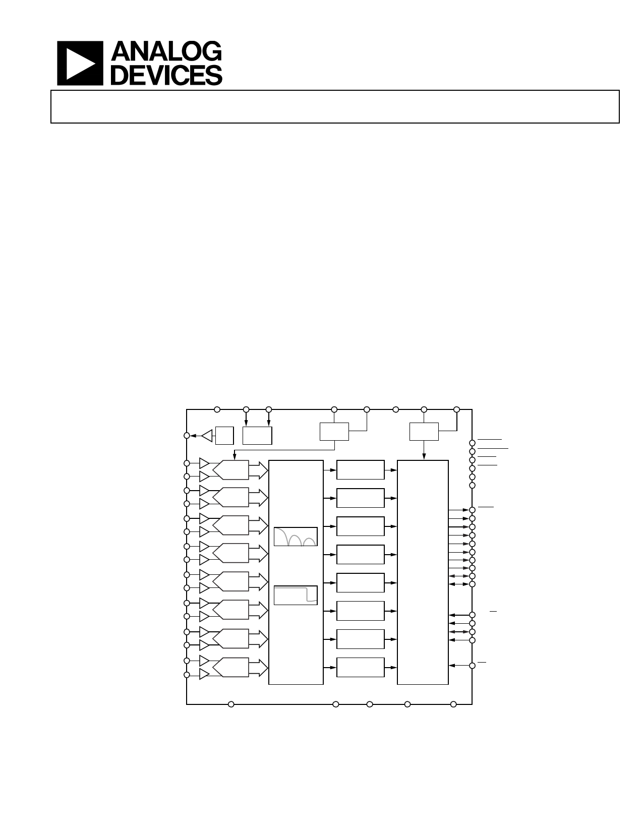
FUNCTIONAL BLOCK DIAGRAM
AVDD1A,
AVDD1B REFx+ REFx–
AVDD2A, REGCAPA,
AVDD2B REGCAPB DGND IOVDD DREGCAP
BUFFERED
VCM
VCM
VCM
PRECHARGE
×8 REFERENCE
BUFFERS
1.8V
LDO
AIN0+
CH 0
AIN0–
AIN1+
CH 1
AIN1–
AIN2+
CH 2
AIN2–
AIN3+
CH 3
AIN3–
AIN4+
CH 4*
AIN4–
AIN5+
CH 5*
AIN5–
AIN6+
CH 6*
AIN6–
P
P
P
P
P
P
P
P
P
P
P
P
P
P
Σ-Δ
ADC
Σ-Δ
ADC
Σ-Δ
ADC
Σ-Δ
ADC
Σ-Δ
ADC
Σ-Δ
ADC
Σ-Δ
ADC
DIGITAL
FILTER
ENGINE
SINC5
LOW LATENCY
FILTER
WIDEBAND
LOW RIPPLE
FILTER
OFFSET,
GAIN PHASE
CORRECTION
OFFSET,
GAIN PHASE
CORRECTION
OFFSET,
GAIN PHASE
CORRECTION
OFFSET,
GAIN PHASE
CORRECTION
OFFSET,
GAIN PHASE
CORRECTION
OFFSET,
GAIN PHASE
CORRECTION
OFFSET,
GAIN PHASE
CORRECTION
1.8V
LDO
ADC
OUTPUT
DATA
SERIAL
INTERFACE
SPI
CONTROL
INTERFACE
SYNC_IN
SYNC_OUT
START
RESET
FORMAT1*
FORMAT0
DRDY
DCLK
DOUT0
DOUT1
DOUT2
DOUT3
DOUT4*
DOUT5*
DOUT6*, DIN
DOUT7*
ST0/CS
ST1*/SCLK
DEC0/SDO
DEC1/SDI
AIN7+
CH 7*
AIN7–
P
Σ-Δ
P ADC
×16 ANALOG INPUT
PRECHARGE BUFFERS (P)
OFFSET,
GAIN PHASE
CORRECTION
AD7768/AD7768-4
PIN/SPI
AVSS
XTAL2/MCLK
*THESE CHANNELS/PINS EXIST ONLY ON THE AD7768.
Figure 1.
XTAL1
MODE3/GPIO3 FILTER/GPIO4
TO
MODE0/GPIO0
Rev. A
Document Feedback
Information furnished by Analog Devices is believed to be accurate and reliable. However, no
responsibility is assumed by Analog Devices for its use, nor for any infringements of patents or other
rights of third parties that may result from its use. Specifications subject to change without notice. No
license is granted by implication or otherwise under any patent or patent rights of Analog Devices.
Trademarksandregisteredtrademarksarethepropertyoftheirrespectiveowners.
One Technology Way, P.O. Box 9106, Norwood, MA 02062-9106, U.S.A.
Tel: 781.329.4700
©2016 Analog Devices, Inc. All rights reserved.
Technical Support
www.analog.com
1 page 
Data Sheet
GENERAL DESCRIPTION
The AD7768/AD7768-4 are 8-channel and 4-channel,
simultaneous sampling sigma-delta (Σ-Δ) analog-to-digital
converters (ADCs), respectively, with a Σ-Δ modulator and digital
filter per channel, enabling synchronized sampling of ac and dc
signals.
The AD7768/AD7768-4 achieve 108 dB dynamic range at a
maximum input bandwidth of 110.8 kHz, combined with typical
performance of ±2 ppm INL, ±50 µV offset error, and ±30 ppm
gain error.
The AD7768/AD7768-4 user can trade off input bandwidth,
output data rate, and power dissipation, and select one of three
power modes to optimize for noise targets and power
consumption. The flexibility of the AD7768/AD7768-4 allows
them to become reusable platforms for low power dc and high
performance ac measurement modules.
The AD7768/AD7768-4 have three modes: fast mode (256 kSPS
maximum, 110.8 kHz input bandwidth, 51.5 mW per channel),
median mode (128 kSPS maximum, 55.4 kHz input bandwidth,
27.5 mW per channel) and eco mode (32 kSPS maximum,
13.8 kHz input bandwidth, 9.375 mW per channel).
The AD7768/AD7768-4 offer extensive digital filtering
capabilities, such as a wideband, low ±0.005 dB pass-band
ripple, antialiasing low-pass filter with sharp roll-off, and
105 dB stop band attenuation at the Nyquist frequency.
Frequency domain measurements can use the wideband linear
phase filter. This filter has a flat pass band (±0.005 dB ripple)
from dc to 102.4 kHz at 256 kSPS, from dc to 51.2 kHz at
128 kSPS, or from dc to 12.8 kHz at 32 kSPS.
The AD7768/AD7768-4 also offer sinc response via a sinc5
filter, a low latency path for low bandwidth, and low noise
measurements. The wideband and sinc5 filters can be selected
and run on a per channel basis.
AD7768/AD7768-4
Within these filter options, the user can improve the dynamic
range by selecting from decimation rates of ×32, ×64, ×128,
×256, ×512, and ×1024. The ability to vary the decimation
filtering optimizes noise performance to the required input
bandwidth.
Embedded analog functionality on each ADC channel makes
design easier, such as a precharge buffer on each analog input
that reduces analog input current and a reference precharge
buffer per channel reduces input current and glitches on the
reference input terminals.
The device operates with a 5 V AVDD1A and AVDD1B supply,
a 2.25 V to 5.0 V AVDD2A and AVDD2B supply, and a 2.5 V to
3.3 V or 1.8 V IOVDD supply (see the 1.8 V IOVDD Operation
section for specific requirements for operating at 1.8 V IOVDD).
The device requires an external reference; the absolute input
reference voltage range is 1 V to AVDD1 − AVSS.
For the purposes of clarity within this document, the AVDD1A
and AVDD1B supplies are referred to as AVDD1 and the AVDD2A
and AVDD2B supplies are referred to as AVDD2. For the negative
supplies, AVSS refers to the AVSS1A, AVSS1B, AVSS2A,
AVSS2B, and AVSS pins.
The specified operating temperature range is −40°C to +105°C.
The device is housed in a 10 mm × 10 mm 64-lead LQFP package
with a 12 mm × 12 mm printed circuit board (PCB) footprint.
Throughout this data sheet, multifunction pins, such as
XTAL2/MCLK, are referred to either by the entire pin name or
by a single function of the pin, for example MCLK, when only
that function is relevant.
Rev. A | Page 5 of 99
5 Page 
Data Sheet
Parameter
Eco
Sinc5 Filter
Fast
Median
Eco
AD7768-4
Wideband Filter
Fast
Median
Eco
Test Conditions/Comments
AVDD1 = 5 V, AVDD2 = IOVDD = 2.5 V,
reference precharge buffers off2
AVDD1 = 5 V, AVDD2 = IOVDD = 3.3 V,
reference precharge buffers on2
AVDD1 = 5.5 V, AVDD2 = 5.5 V, IOVDD =
3.6 V, reference precharge buffers off
Min
AVDD1 = 5 V, AVDD2 = IOVDD = 2.5 V,
reference precharge buffers off2
AVDD1 = 5 V, AVDD2 = IOVDD = 3.3 V,
reference precharge buffers on2
AVDD1 = 5.5 V, AVDD2 = 5.5 V, IOVDD =
3.6 V, reference precharge buffers off
AVDD1 = 5 V, AVDD2 = IOVDD = 2.5 V,
reference precharge buffers off2
AVDD1 = 5 V, AVDD2 = IOVDD = 3.3 V,
reference precharge buffers on2
AVDD1 = 5.5 V, AVDD2 = 5.5 V, IOVDD =
3.6 V, reference precharge buffers off
AVDD1 = 5 V, AVDD2 = IOVDD = 2.5 V,
reference precharge buffers off2
AVDD1 = 5 V, AVDD2 = IOVDD = 3.3 V,
reference precharge buffers on2
AVDD1 = 5.5 V, AVDD2 = 5.5 V, IOVDD =
3.6 V, reference precharge buffers off
AVDD1 = 5 V, AVDD2 = IOVDD = 2.5 V,
reference precharge buffers off
AVDD1 = 5 V, AVDD2 = IOVDD = 3.3 V,
reference precharge buffers on
AVDD1 = 5.5 V, AVDD2 = 5.5 V, IOVDD =
3.6 V, reference precharge buffers off2
SPI mode only; AVDD1 = 5.5 V, AVDD2 =
5.5 V, IOVDD = 3.6 V, reference precharge
buffers off, Channel Mode A set to sinc5
filter8
Rev. A | Page 11 of 99
Typ
75
107
124
325
475
501
175
260
277
65
95
108
235
336
360
337
127
181
198
186
49
66
77
73
AD7768/AD7768-4
Max Unit
85 mW
118 mW
137 mW
355 mW
525 mW
545 mW
195 mW
285 mW
304 mW
72 mW
105 mW
120 mW
mW
mW
392 mW
368 mW
mW
mW
218 mW
205 mW
mW
mW
87 mW
83 mW
11 Page | ||
| Páginas | Total 30 Páginas | |
| PDF Descargar | [ Datasheet AD7768.PDF ] | |
Hoja de datos destacado
| Número de pieza | Descripción | Fabricantes |
| AD776 | 16-Bit 100 kSPS Oversampling ADC | Analog Devices |
| AD7760 | 2.5 MSPS 20-Bit ADC | Analog Devices |
| AD7761 | Simultaneous Sampling ADC | Analog Devices |
| AD7762 | With On-Chip Buffer 625 KSPS | Analog Devices |
| Número de pieza | Descripción | Fabricantes |
| SLA6805M | High Voltage 3 phase Motor Driver IC. |
Sanken |
| SDC1742 | 12- and 14-Bit Hybrid Synchro / Resolver-to-Digital Converters. |
Analog Devices |
|
DataSheet.es es una pagina web que funciona como un repositorio de manuales o hoja de datos de muchos de los productos más populares, |
| DataSheet.es | 2020 | Privacy Policy | Contacto | Buscar |