|
|
PDF EM78P467C Data sheet ( Hoja de datos )
| Número de pieza | EM78P467C | |
| Descripción | 8-BIT MICRO-CONTROLLER | |
| Fabricantes | EMC | |
| Logotipo |  |
|
Hay una vista previa y un enlace de descarga de EM78P467C (archivo pdf) en la parte inferior de esta página. Total 20 Páginas | ||
|
No Preview Available !
DESCRIPTION
EM78P267/467A/B/C
8-BIT MICRO-CONTROLLER FOR CONSUMER PRODUCT
Preliminary
The EM78P267/467A/B/C is an 8-bit microprocessor with low-power, high speed CMOS technology. There
are 4Kx13 bits Electical One Time Programmable Read Only Memory (OTP-ROM) within it. It provides 1
Protect bit and 6 One-time Programmable Option bits to protect the OTP memory code from any external access
as well as the user's options.
The OTP ROM will be incorporated into EM78P267/467A/B/C 8-bit microcontroller instead of it's original
memory. The user's development program can be easily programmed into or verify from this OTP memory by
using EMC OTP PROGRAMMER.
FEATURES
• Operating voltage range: 2.5V~5.5V
• Available in temperature range: 0°C~70°C
• Operating frequency range:
Crystal Type: DC~20MHz at 5V
DC~8MHz at 3V
RC Type:
DC~4MHz at 5V
DC~4MHz at 3V
• 2Kx13 on chip ROM (EM78267A/B/C)
• 4Kx13 on chip ROM (EM78467A/B/C)
• 9 special function registers
• 148x8 general purpose registers (SRAM)
• 3 bi-directional tri-state I/O ports (20 I/O pins for EM78P267/467A) (24 I/O pins for EM78P267/467B)
(22 I/O pins for EM78P267/467C)
• 5 level stack for subroutine nesting
• 8-bit real time clock/counter (TCC) with selective signal sources and trigger edges, and with overflow interrupt
• Selectable oscillator options:
XTAL1 type (High frequency)
XTAL2 type (32.768KHz)
RC type
External clock input
• Two oscillator periods per instruction cycle
• Power down mode
• Programmable wake up from sleep circuit on I/O ports
• Programmable free running on-chip watchdog timer
• Ten pull-up and wake-up pins
• Two open-drain pins
• Two R-option pins
• Interrupt function available
• 28 pin DIP, SOIC, SSOP
(EM78P267/467A)
28 pin SOIC
(EM78P267/467C)
* This specification are subject to be changed without notice.
9.5.1997 1
1 page 
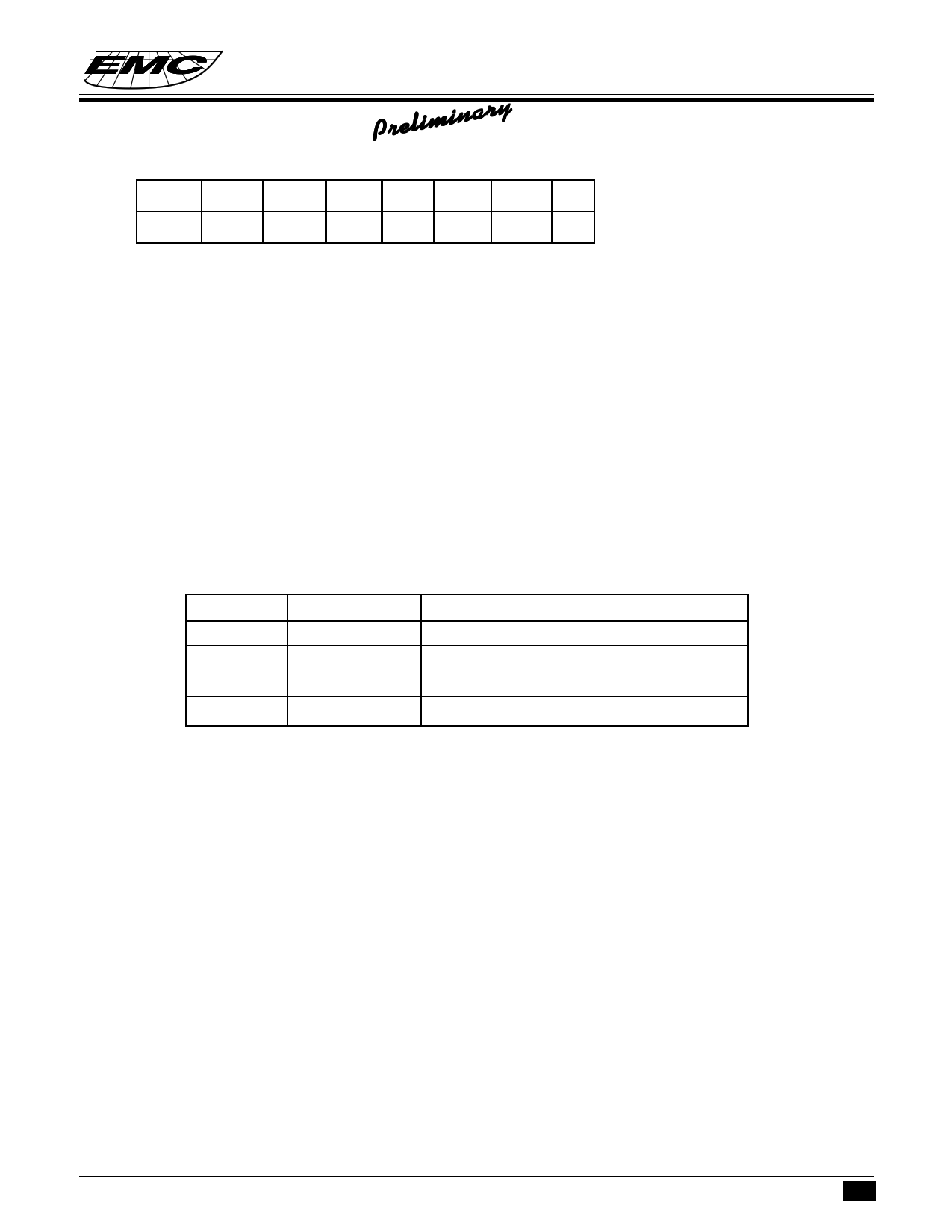
R3 (Status Register)
EM78P267/467A/B/C
8-BIT MICRO-CONTROLLER FOR CONSUMER PRODUCT
Preliminary
76
5 43210
GP PS1 PS0 T P Z DC C
• Bit 0 ( C ) Carry flag
• Bit 1 (DC) Auxiliary carry flag
• Bit 2 (Z) Zero flag. Set to “1” if the result of an arithmetic or logic operation is zero.
• Bit 3 (P) Power down bit. Set to 1 during power on or by a “WDTC” command and reset to 0 by a “SLEP”
command.
• Bit 4 (T) Time-out bit. Set to 1 by the “SLEP” and “WDTC” command, or during power up and reset to 0 by
WDT time-out.
• Bits 5 (PS0) ~ 6 (PS1) Page select bits. PS0~PS1 are used to preselect a program memory page. When executing
a “JMP”, “CALL”, or other instruction which causes the program counter to be changed (e.g. MOV R2,A),
PS0~PS1 are loaded into the 11th and 12th bits of the program counter, selecting one of the available program
memory pages. Note that RET (RETL, RETI) instruction does not change the PS0~PS1 bits. That is, the return
will be always to the page from where the subroutine was called, regardless of the current setting of PS0~PS1
bits.
PS1 PS0
00
01
10
11
Program memory page [Address]
Page 0 [000-3FF]
Page 1 [400-7FF]
Page 2 [800-BFF]
Page 3 [C00-FFF]
• Bit 7 (GP) General read/write bit.
R4 (RAM Select Register)
• Bits 0~5 are used to select the registers (address: 00~3F) in the indirect addressing mode.
• Bits 6~7 determine which bank is activated among the 4 banks.
• If no indirect addressing is used, the RSR can be used as an 8-bit wide general purpose read/write register.
• See the configuration of the data memory in Fig. 4.
R5 (Port 5)
• EM78P267/467A: Only low order 4 bits are used in R5. The high order 4 bits of R5 will be read as “0”.
• EM78P267/467B/C: All 8 bits are used in R5.
R6~R7 (Port 6 ~ Port 7)
• Two 8-bit I/O registers.
* This specification are subject to be changed without notice.
9.5.1997 5
5 Page 
EM78P267/467A/B/C
8-BIT MICRO-CONTROLLER FOR CONSUMER PRODUCT
Preliminary
CLK(=Fosc/2)
Data Bus
TCC
Pin
TE
WDT
WTE
(in IOCE)
0
M
U
1X
1M
U
0X
SYNC
2 cycles
TCC(R1)
TS PAB
TCC overflow interrupt
0M
U
1X
PAB
8-bit Counter
8-to-1 MUX
01
MUX
PSR0~PSR2
PAB
WDT timeout
Fig. 6 Block diagram of TCC WDT
PCRD
Q PR D
CLK
Q CL
PCWR
PORT
0M
1U
X
Q PR D
CLK
Q CL
PDWR
PDRD
IOD
Fig. 7(a) The circuit of I/O port and I/O control register
* This specification are subject to be changed without notice.
9.5.1997 11
11 Page | ||
| Páginas | Total 20 Páginas | |
| PDF Descargar | [ Datasheet EM78P467C.PDF ] | |
Hoja de datos destacado
| Número de pieza | Descripción | Fabricantes |
| EM78P467 | 8-BIT MICRO-CONTROLLER | EMC |
| EM78P467A | 8-BIT MICRO-CONTROLLER | EMC |
| EM78P467B | 8-BIT MICRO-CONTROLLER | EMC |
| EM78P467C | 8-BIT MICRO-CONTROLLER | EMC |
| Número de pieza | Descripción | Fabricantes |
| SLA6805M | High Voltage 3 phase Motor Driver IC. |
Sanken |
| SDC1742 | 12- and 14-Bit Hybrid Synchro / Resolver-to-Digital Converters. |
Analog Devices |
|
DataSheet.es es una pagina web que funciona como un repositorio de manuales o hoja de datos de muchos de los productos más populares, |
| DataSheet.es | 2020 | Privacy Policy | Contacto | Buscar |
