|
|
|
PDF GS9025A Data sheet ( Hoja de datos )
| Número de pieza | GS9025A | |
| Descripción | Serial Digital Receiver | |
| Fabricantes | GENNUM | |
| Logotipo | ||
Hay una vista previa y un enlace de descarga de GS9025A (archivo pdf) en la parte inferior de esta página. Total 18 Páginas | ||
|
No Preview Available !
GENLINX ™II GS9025A
Serial Digital Receiver
FEATURES
• SMPTE 259M compliant
• operational to 540Mb/s
• automatic cable equalization (typically greater than
350m of high quality cable at 270Mb/s)
• adjustment-free operation
• auto-rate selection (5 rates) with manual override
• single external VCO resistor for operation with five
input data rates
• data rate indication output
• serial data outputs muted and serial clock remains
active when input data is lost
• operation independent of SAV/EAV sync signals
• signal strength indicator output
• carrier detect with programmable threshold level
• power savings mode (output serial clock disable)
• Pb-free and Green
APPLICATIONS
Cable equalization plus clock and data recovery for all high
speed serial digital interface applications involving SMPTE
259M and other data standards.
DATA SHEET
DESCRIPTION
The GS9025A provides automatic cable equalization and
high performance clock and data recovery for serial digital
signals. The GS9025A receives either single-ended or
differential serial digital data and outputs differential clock
and retimed data signals at PECL levels (800mV). The on-
board cable equalizer provides up to 40dB of gain at
200MHz which typically results in equalization of greater
than 350m of high quality cable at 270Mb/s.
The GS9025A operates in either auto or manual data rate
selection mode. In both modes, the GS9025A requires only
one external resistor to set the VCO centre frequency and
provides adjustment free operation.
The GS9025A has dedicated pins to indicate signal
strength/carrier detect, LOCK and data rate. Optional
external resistors allow the carrier detect threshold level to
be customized to the user's requirement. In addition, the
GS9025A provides an 'Output Eye Monitor Test'
(OEM_TEST) for diagnostic testing of signal integrity after
equalization, prior to reslicing. The serial clock outputs can
also be disabled to reduce power. The GS9025A operates
from a single +5 or -5 volt supply.
ORDERING INFORMATION
PART NUMBER
GS9025ACQM
GS9025ACTM
GS9025ACQME3
GS9025ACTME3
PACKAGE
44 pin MQFP Tray
44 pin MQFP Tape
44 pin MQFP Tray
44 pin MQFP Tape
TEMPERATURE
0°C to 70°C
0°C to 70°C
0°C to 70°C
0°C to 70°C
Pb-FREE AND GREEN
No
No
Yes
Yes
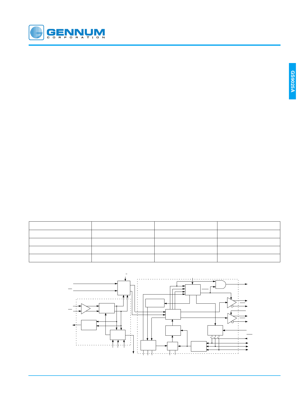
A/D
DDI
ANALOG
CARRIER DETECT
DDI
DIGITAL
MUX
PHASELOCK
HARMONIC
SDI +
SDI --
VARIABLE
GAIN EQ
STAGE
OEM_TEST
EYE
MONITOR
AUTO EQ
CONTROL
FREQUENCY
ACQUISITION
PHASE
DETECTOR
DIVISION
+-
AGC CAP CD_ADJ
CHARGE
PUMP
VCO
SSI/CD LF+ LFS LF-
CBG RVCO
BLOCK DIAGRAM
COSC
LOGIC MUTE
3 BIT
COUNTER
DECODER
LOCK
SDO
SDO
CLK_EN
SCO
SCO
SMPTE
AUTO/MAN
SS0
SS1
SS2
Revision Date: August 2005
GENNUM CORPORATION P.O. Box 489, Stn. A, Burlington, Ontario, Canada L7R 3Y3
Tel. +1 (905) 632-2996 Fax. +1 (905) 632-5946 E-mail: [email protected]
www.gennum.com
Document No. 522 - 75 - 05
1 page 
PIN CONNECTIONS
DDI
DDI
VCC_75
VCC
VEE
SDI
SDI
VCC
VEE
CD_ADJ
AGC-
44 43 42 41 40 39 38 37 36 35 34
1 33
2 32
3 31
4 30
5
GS9025A
29
6
TOP VIEW
28
7 27
8 26
9 25
10 24
11 23
12 13 14 15 16 17 18 19 20 21 22
VEE
SDO
SDO
VEE
SCO
SCO
VEE
AUTO/MAN
SS0
SS1
SS2
PIN DESCRIPTIONS
NUMBER
SYMBOL TYPE
DESCRIPTION
1, 2
DDI/DDI
I Digital data inputs (Differential ECL/PECL).
3, 44
VCC_75
I Power supply connection for internal 75Ω pull-up resistors connected to DDI/DDI.
4, 8, 13, 22, 35
5, 9, 14, 18, 27,
30, 33, 34, 37
VCC
VEE
I Most positive power supply connection.
I Most negative power supply connection.
6, 7
SDI/SDI
I Differential analog data inputs.
10
CD_ADJ
I Carrier detect threshold adjust.
11, 12
AGC-, AGC+ I External AGC capacitor. VCOMMON MODE=2.7V TYP.
15 LF+ I Loop filter component connection.
16 LFS I Loop filter component connection.
17 LF- I Loop filter component connection.
19
RVCO_RTN
I Frequency setting resistor return connection.
20
RVCO
I Frequency setting resistor connection.
21
CBG
I Internal bandgap voltage filter capacitor.
23, 24, 25
SS[2:0]
I/O Data rate indication (auto mode) or data rate select (manual mode). TTL/CMOS
compatible I/O. In auto mode, these pins can be left unconnected.
26
AUTO/MAN
I Auto or manual mode select. TTL/CMOS compatible input.
GENNUM CORPORATION
5 of 18
522 - 75 - 05
5 Page 
800
700
600
500
400 ƒH
300
200
100
00
200 400
ƒL
SMPTE=1
SSO=1
600 800 1000 1200 1400 1600 1800
RVCO (Ω)
Fig. 19 RVCO vs. VCO Centre Frequency
The recommended RVCO value for auto rate SMPTE 259M
applications is 365Ω.
The VCO and an internal divider generate the PLL clock.
Divider moduli of 1, 2, and 4 allow the PLL to lock to data
rates from 143Mb/s to 540Mb/s. The divider modulus is set
by the AUTO/MAN, SMPTE, and SS[2:0] pins (for further
details, see section 2.4, Auto/Manual Data Rate Select). In
addition, a manually selectable modulus 8 divider allows
operation at data rates as low as 30Mb/s.
When the input data stream is removed for an excessive
period of time (see AC Electrical Characteristics table), the
VCO frequency can drift from the previously locked
frequency to the limits shown in Table1.
TABLE 1: Frequency Drift Range (when PLL loses lock)
LOSES LOCK FROM
MIN (%)
MAX(%)
143Mb/s lock
-21 21
177Mb/s lock
-12 26
270Mb/s lock
-13 28
360 Mb/s lock -13 24
540 Mb/s lock -13 28
2.1.2 Phase Detector
The phase detector compares the phase of the PLL clock
with the phase of the incoming data signal and generates
error correcting timing pulses. The phase detector design
provides a linear transfer function which maximizes the
input jitter tolerance of the PLL.
2.1.3 Charge Pump
The charge pump takes the phase detector output timing
pulses and creates a charge packet that is proportional to
the system phase error. A unique differential charge pump
design ensures that the output phase does not drift when
data transitions are sparse. This makes the GS9025A ideal
for SMPTE 259M applications where pathological signals
have data transition densities of 0.05.
2.1.4 Loop Filter
The loop filter integrates the charge pump packets and
produces a VCO control voltage. The loop filter is
comprised of three external components which are
connected to pins LF+, LFS, and LF-. The loop filter design
is fully differential which increases the GS9025’s immunity to
PCB board noise.
The loop filter components are critical in determining the
loop bandwidth and damping of the PLL. Choosing these
component values is discussed in detail in section 2.9, PLL
Design Guidelines. Recommended values for SMPTE 259M
applications are shown in the Typical Application Circuit.
2.2 Frequency Acquisition
The core PLL is able to lock if the incoming data rate and
the PLL clock frequency are within the PLL capture range
(which is slightly larger than the loop bandwidth). To assist
the PLL to lock to data rates outside of the capture range,
the GS9025A uses a frequency acquisition circuit.
The frequency acquisition circuit sweeps the VCO control
voltage so that the VCO frequency changes from -10% to
+10% of the centre frequency. Figure 20 shows a typical
sweep waveform.
tswp
tsys
VLF
A
Tcycle
Tcycle = tswp + tsys
Fig. 20 Typical Sweep Waveform
The VCO frequency starts at point A and sweeps up
attempting to lock. If lock is not established during the up
sweep, the VCO is then swept down. The probability of
locking within one cycle period is greater than 0.999. If the
system does not lock within one cycle period, it will attempt
to lock in the subsequent cycle. In manual mode, the
divider modulus is fixed for all cycles. In auto mode, each
subsequent cycle is based on a different divider moduli as
determined by the internal 3-bit counter.
The average sweep time, tswp, is determined by the loop
filter component, CLF1, and the charge pump current, ΙCP:
tSWP
=
4----C-----L---F---1-
3ICP
The nominal sweep time is approximately 121µs when
CLF1 = 15nF and ΙCP = 165µA (RVCO = 365Ω).
An internal system clock determines tsys (see section 2.3,
Logic Circuit).
GENNUM CORPORATION
11 of 18
522 - 75 - 05
11 Page | ||
| Páginas | Total 18 Páginas | |
| PDF Descargar | [ Datasheet GS9025A.PDF ] | |
Hoja de datos destacado
| Número de pieza | Descripción | Fabricantes |
| GS9025A | Serial Digital Receiver | ETC |
| GS9025A | Serial Digital Receiver | GENNUM |
| GS9025ACQM | Serial Digital Receiver | ETC |
| GS9025ACQM | Serial Digital Receiver | GENNUM |
| Número de pieza | Descripción | Fabricantes |
| SLA6805M | High Voltage 3 phase Motor Driver IC. |
Sanken |
| SDC1742 | 12- and 14-Bit Hybrid Synchro / Resolver-to-Digital Converters. |
Analog Devices |
|
DataSheet.es es una pagina web que funciona como un repositorio de manuales o hoja de datos de muchos de los productos más populares, |
| DataSheet.es | 2020 | Privacy Policy | Contacto | Buscar |