|
|
|
PDF EN5337QI Data sheet ( Hoja de datos )
| Número de pieza | EN5337QI | |
| Descripción | 3A PowerSoC Voltage Mode Synchronous Buck PWM DC-DC Converter | |
| Fabricantes | Altera | |
| Logotipo | ||
Hay una vista previa y un enlace de descarga de EN5337QI (archivo pdf) en la parte inferior de esta página. Total 16 Páginas | ||
|
No Preview Available !
Enpirion® Power Datasheet
EN5337QI 3A PowerSoC
Voltage Mode Synchronous
Buck PWM DC-DC Converter
with Integrated Inductor
FDescription
The EN5337QI is a Power Supply on a Chip
(PowerSoC) DC-DC converter. It integrates
MOSFET switches, all small-signal circuits,
compensation, and the inductor in an advanced
4mm x 7mm QFN package.
The EN5337QI is specifically designed to meet
the precise voltage and fast transient
requirements of present and future high-
performance, low-power processor, DSP, FPGA,
memory boards, and system level applications in
distributed power architectures. Advanced circuit
techniques, ultra high switching frequency, and
very advanced, high-density, integrated circuit
and proprietary inductor technology deliver high-
quality, ultra compact, non-isolated DC-DC
conversion.
The Altera Enpirion solution significantly helps in
system design and productivity by offering greatly
simplified board design, layout and
manufacturing requirements. In addition, a
reduction in the number of vendors required for
the complete power solution helps to enable an
overall system cost savings.
All Altera Enpirion products are RoHS compliant
and lead-free manufacturing environment
compatible.
RA 0402
CA 0402
RB 0402
0402
Soft Start Cap
Features
• Integrated Inductor, MOSFETS, Controller
• Total Power Solution ≈ 75mm2
• Minimal external components.
• 3A Continuous Output Current Capability
• 5MHz operating frequency. Switching
frequency can be phase locked to an external
clock.
• High efficiency, up to 92%.
• Wide input voltage range of 2.375V to 5.5V.
• Output Enable pin and Power OK signal.
• Programmable soft-start time.
• Under Voltage Lockout, Over Current, Short
Circuit and Thermal Protection.
• RoHS compliant, MSL level 3, 260C reflow.
Applications
• Point of load regulation for low-power
processors, network processors, DSPs,
FPGAs, and ASICs
• Noise sensitive applications such as A/V, RF
and Gbit I/O
• Low voltage, distributed power architectures
with 2.5V, 3.3V or 5V rails
• Computing, Networking, DSL, STB, DVR,
DTV, iPC
• Ripple sensitive applications
• Beat frequency sensitive applications
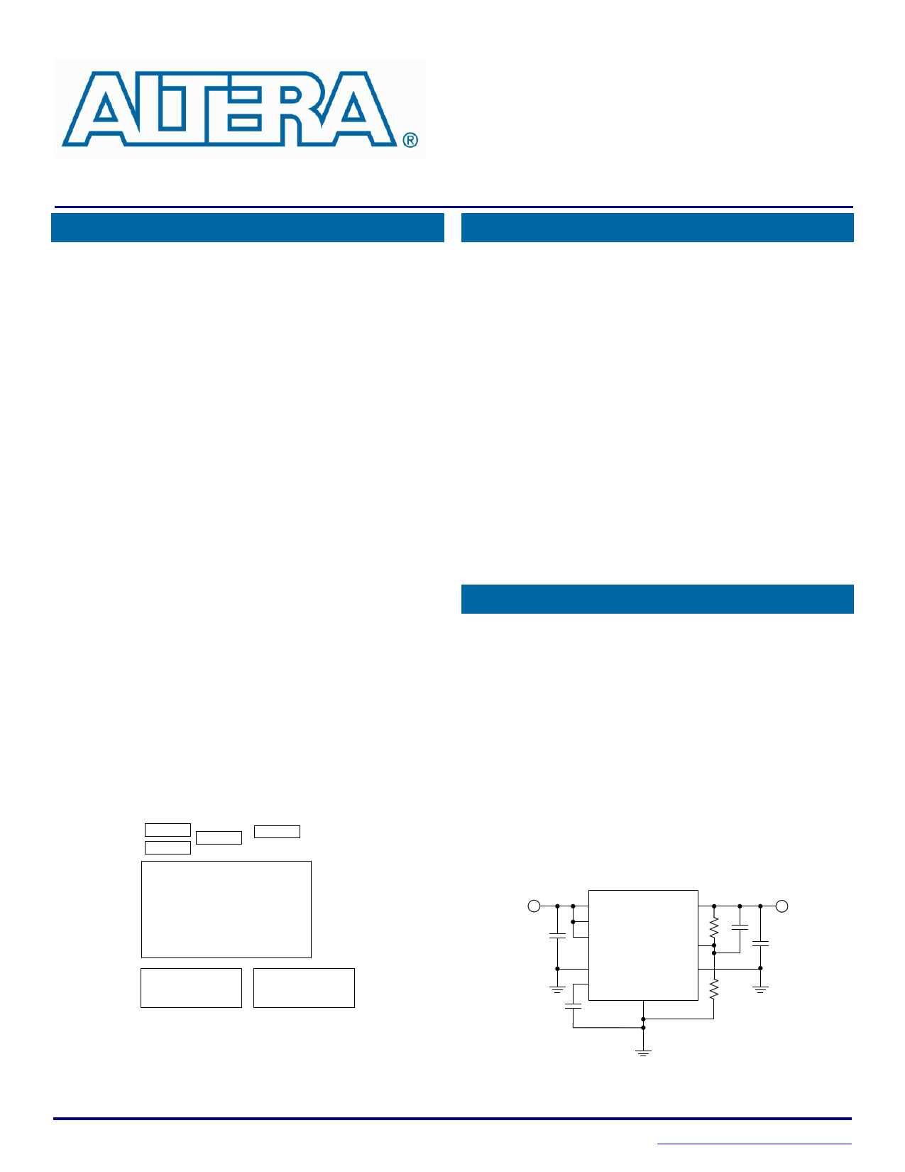
EN5337QI
Output Cap Input Cap
47uF/1206 22uF/1206
VIN
22µF
1206
PVIN
ENA
AVIN
VOUT
XFB
PGND
SS
AGND
PGND
RA
CA
RB
VOUT
47µF
1206
Figure 1: Total Solution Footprint (Not to scale)
Total Area ≈ 75 mm2
Figure 2: Typical Application Schematic
02638
July 15, 2015
www.altera.com/enpirion
Rev H
1 page 
Note 1: Parameter guaranteed by design
Typical Performance Characteristics
EN5337QI
90
80
70
60 VIN = 3.3V
50
40
30
0 0.5 1 1.5 2 2.5 3
Load (Amps)
Efficiency VIN = 3.3V
VOUT (From top to bottom) = 2.5, 1.8, 1.2, 1.0, 0.75V
90
80
70
60
50 VIN = 5V
40
30
20
0 0.5 1 1.5 2 2.5 3
Load (Amps)
Efficiency VIN = 5.0V
VOUT (From top to bottom) = 3.3, 2.5, 1.8, 1.2, 1.0, 0.75V
20 MHz BW limit
Output Ripple: VIN = 3.3V, VOUT = 1.2V, Iout = 3A
CIN = 22µF, COUT = 47µF/1206 + 10uF/0805
500 MHz BW
Output Ripple: VIN = 3.3V, VOUT = 1.2V, Iout = 3A
CIN = 22µF, COUT = 47µF/1206 + 10uF/0805
20 MHz BW limit
500 MHz BW
Output Ripple: VIN = 5V, VOUT = 1.2V, Iout = 3A
CIN = 22µF, COUT = 47µF/1206 + 10uF/0805
Output Ripple: VIN = 5V, VOUT = 1.2V, Iout = 3A
02638
5
July 15, 2015
www.altera.com/enpirion
Rev H
5 Page 
capacitors are required with X5R or X7R rated
dielectric formulation. Y5V or equivalent
dielectric formulations must not be used as
these lose too much capacitance with
frequency, temperature and bias voltage.
Output ripple voltage is determined by the
aggregate output capacitor impedance. Output
impedance, denoted as Z, is comprised of
effective series resistance, ESR, and effective
series inductance, ESL:
Z = ESR + ESL
Placing output capacitors in parallel reduces
the impedance and will hence result in lower
ripple voltage.
1 = 1 + 1 + ... + 1
ZTotal Z1 Z 2
Zn
Typical Ripple Voltages
Output Capacitor
Configuration
1 x 47 uF
47 uF + 10 uF
Typical Output Ripple (mVp-p)
(as measured on EN5335QI
Evaluation Board)
30
15
EN5337QI
Recommended Output Capacitors
Description
47uF, 6.3V, 20%
X5R, 1206
(1 capacitor needed)
10uF, 6.3V, 10%
X5R, 0805
(Optional 1 capacitor in
parallel with 47uF above)
MFG
Murata
Taiyo Yuden
Murata
Taiyo Yuden
P/N
GRM31CR60J476ME19L
JMK212BJ476ML-T
GRM21BR60J106KE19L
JMK212BJ106KG-T
Power-Up Sequencing
During power-up, ENABLE should not be
asserted before PVIN, and PVIN should not be
asserted before AVIN. Tying all three pins
together meets these requirements.
Thermal Considerations
The Altera Enpirion EN5337QI DC-DC
converter is packaged in a 7 x 4 x 1.85mm 38-
pin QFN package. The QFN package is
constructed with copper lead frames that have
exposed thermal pads. The recommended
maximum junction temperature for continuous
operation is 125°C. Continuous operation
above 125°C will reduce long-term reliability.
The device has a thermal overload protection
circuit designed to shut it off at an approximate
junction temperature value of 150°C.
The silicon is mounted on a copper thermal
pad that is exposed at the bottom of the
package. The thermal resistance from the
silicon to the exposed thermal pad is very low.
In order to take advantage of this low
resistance, the exposed thermal pad on the
package should be soldered directly on to a
copper ground pad on the printed circuit board
(PCB). The PCB then acts as a heat sink. In
order for the PCB to be an effective heat sink,
the device thermal pad should be coupled to
copper ground planes or special heat sink
structures designed into the PCB (refer to the
recommendations at the end of this note).
The junction temperature, TJ, is calculated
from the ambient temperature, TA, the device
power dissipation, PD, and the device junction-
to-ambient thermal resistance, θJA in °C/W::
TJ = TA + (PD)(θJA)
The junction temperature, TJ, can also be
expressed in terms of the device case
temperature, TC, and the device junction-to-
case thermal resistance, θJC in °C/W, as
follows:
TJ = TC + (PD)(θJC)
The device case temperature, TC, is the
temperature at the center of the exposed
thermal pad at the bottom of the package.
The device junction-to-ambient and junction-to-
02638
11
July 15, 2015
www.altera.com/enpirion
Rev H
11 Page | ||
| Páginas | Total 16 Páginas | |
| PDF Descargar | [ Datasheet EN5337QI.PDF ] | |
Hoja de datos destacado
| Número de pieza | Descripción | Fabricantes |
| EN5337QI | 3A PowerSoC Voltage Mode Synchronous Buck PWM DC-DC Converter | Altera |
| Número de pieza | Descripción | Fabricantes |
| SLA6805M | High Voltage 3 phase Motor Driver IC. |
Sanken |
| SDC1742 | 12- and 14-Bit Hybrid Synchro / Resolver-to-Digital Converters. |
Analog Devices |
|
DataSheet.es es una pagina web que funciona como un repositorio de manuales o hoja de datos de muchos de los productos más populares, |
| DataSheet.es | 2020 | Privacy Policy | Contacto | Buscar |