|
|
|
PDF AOB403 Data sheet ( Hoja de datos )
| Número de pieza | AOB403 | |
| Descripción | P-Channel Enhancement Mode Field Effect Transistor | |
| Fabricantes | Alpha & Omega Semiconductors | |
| Logotipo | ||
Hay una vista previa y un enlace de descarga de AOB403 (archivo pdf) en la parte inferior de esta página. Total 5 Páginas | ||
|
No Preview Available !
AOB403
P-Channel Enhancement Mode Field Effect Transistor
General Description
The AOB403 uses advanced trench technology to
provide excellent RDS(ON), low gate charge and low
gate resistance. With the excellent thermal resistance
of the D2-PAK package, this device is well suited for
high current load applications. Standard product
AOB403 is Pb-free (meets ROHS & Sony 259
specifications). AOB403L is a Green Product ordering
option. AOB403 and AOB403L are electrically
identical.
Features
VDS (V) = -60V
ID = -30A (VGS=-10V)
RDS(ON) < 44mΩ (VGS = -10V ) @ 30A
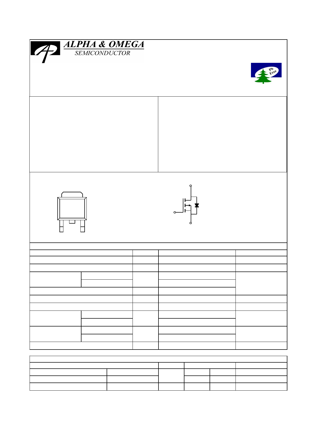
RDS(ON) < 55mΩ (VGS = -4.5V ) @ 20A
TO-263
D2-PAK
D
Top View
Drain Connected to
Tab
G
S
GD S
Absolute Maximum Ratings TA=25°C unless otherwise noted
Parameter
Symbol
Drain-Source Voltage
VDS
Gate-Source Voltage
VGS
Continuous Drain
TC=25°C
Current
TC=100°C
Pulsed Drain Current C
Avalanche Current C
Repetitive avalanche energy L=0.1mH C
ID
IDM
IAR
EAR
TC=25°C
Power Dissipation B TC=100°C
PD
TA=25°C
Power Dissipation A TA=70°C
PDSM
Junction and Storage Temperature Range TJ, TSTG
Maximum
-60
±20
-30
-20
-60
-26
134
83
42
2.2
1.45
-55 to 175
Thermal Characteristics
Parameter
Maximum Junction-to-Ambient A
Maximum Junction-to-Ambient A
Maximum Junction-to-Case C
t ≤ 10s
Steady-State
Steady-State
Symbol
RθJA
RθJC
Typ
10
45
1.35
Max
12
55
1.8
Units
V
V
A
A
mJ
W
W
°C
Units
°C/W
°C/W
°C/W
Alpha & Omega Semiconductor, Ltd.
1 page 
AOB403
TYPICAL ELECTRICAL AND THERMAL CHARACTERISTICS
30
25
tA
=
L⋅ ID
BV − VDD
20
15 TA=25°C
10
0.00001
0.0001
0.001
Time in avalanche, tA (s)
Figure 12: Single Pulse Avalanche capability
100
90
80
70
60
50
40
30
20
10
0
0
25 50 75 100 125 150
TCASE (°C)
Figure 13: Power De-rating (Note B)
175
40
35
30
25
20
15
10
5
0
0
10
1
25 50 75 100 125 150
TCASE (°C)
Figure 14: Current De-rating (Note B)
175
100
90
80 TA=25°C
70
60
50
40
30
20
10
0
0.001 0.01 0.1 1 10 100 1000
Pulse Width (s)
Figure 15: Single Pulse Power Rating Junction-to-
Ambient (Note H)
D=Ton/T
TJ,PK=TA+PDM.ZθJA.RθJA
RθJA=55°C/W
In descending order
D=0.5, 0.3, 0.1, 0.05, 0.02, 0.01, single pulse
0.1
0.01
0.001
0.00001
Single Pulse
PD
Ton
T
0.0001
0.001
0.01
0.1
1
10
Pulse Width (s)
Figure 16: Normalized Maximum Transient Thermal Impedance (Note H)
100
1000
Alpha & Omega Semiconductor, Ltd.
5 Page | ||
| Páginas | Total 5 Páginas | |
| PDF Descargar | [ Datasheet AOB403.PDF ] | |
Hoja de datos destacado
| Número de pieza | Descripción | Fabricantes |
| AOB403 | P-Channel Enhancement Mode Field Effect Transistor | Alpha & Omega Semiconductors |
| AOB403 | P-Channel Enhancement Mode Field Effect Transistor | Alpha & Omega Semiconductors |
| AOB405 | P-Channel Enhancement Mode Field Effect Transistor | Alpha & Omega Semiconductors |
| Número de pieza | Descripción | Fabricantes |
| SLA6805M | High Voltage 3 phase Motor Driver IC. |
Sanken |
| SDC1742 | 12- and 14-Bit Hybrid Synchro / Resolver-to-Digital Converters. |
Analog Devices |
|
DataSheet.es es una pagina web que funciona como un repositorio de manuales o hoja de datos de muchos de los productos más populares, |
| DataSheet.es | 2020 | Privacy Policy | Contacto | Buscar |