|
|
|
PDF CHL8510 Data sheet ( Hoja de datos )
| Número de pieza | CHL8510 | |
| Descripción | 12V High Performance Gate Driver | |
| Fabricantes | International Rectifier | |
| Logotipo | ||
Hay una vista previa y un enlace de descarga de CHL8510 (archivo pdf) en la parte inferior de esta página. Total 15 Páginas | ||
|
No Preview Available !
IR3537
12V High Performance Gate Driver CHL8510
FEATURES
Drives both high‐side and low‐side MOSFETs in a
synchronous buck configuration
Large drivers designed to drive 6nF server class FETs
o Low‐side driver – 4A source / 6A sink
o High‐side driver – 3A source / 4A sink
o Transition times & propagation delays < 20ns
Independent variable gate drive voltage for both
high‐ and low‐side drivers from 4.5V to 13.2V
o Improves efficiency
o Compatible with IR controller VGD feature
Integrated bootstrap diode
o Reduces external component count
Capable of high switching frequencies from 200kHz
up to 1MHz
Configurable PWM modes of operation
o IR Active Tri‐Level (ATL), disables both MOSFETs
in 30ns with no hold‐off time
o Generic Tri‐State PWM with hold‐off
Adaptive non‐overlap protection minimizes diode
conduction time
Input supply under voltage protection
Thermally enhanced 10‐pin DFN package
Lead free RoHS compliant package, MSL level 1
APPLICATIONS
Multiphase synchronous buck converter for
Server and desktop computers using Intel® and
AMD® VR solutions
High efficiency and compact VRM
High current DC/DC converters
DESCRIPTION
The IR3537/CHL8510 is a high efficiency gate driver which
can switch both high‐side and low‐side N‐channel external
MOSFETs in a synchronous buck converter. It is intended
for use with International Rectifier’s Digital PWM
controllers to provide a total voltage regulator (VR)
solution for today’s advanced computing applications.
The IR3537/CHL8510 low‐side driver is capable of rapidly
switching large MOSFETs with low RDS(on) and large input
capacitance used in high efficiency designs.
The IR3537/CHL8510 features individual control of
both the high‐and low‐side gate drive voltages from
4.5V to 13.2V. This enables the optimization of switching
and conduction losses in the external MOSFETs. When
used with IR’s proprietary Variable Gate Drive (VGD)
technology, a significant improvement in efficiency is
observed across the entire load range.
The IR3537/CHL8510 can be configured to drive both the
high‐ and low‐side switches from the unique IR fast Active
Tri‐Level (ATL) PWM signal or a generic tri‐state PWM
mode. The IR ATL mode allows the controller to disable
the high‐ and low‐side FETs in less than 30ns without the
need for a dedicated disable pin. This improves VR
transient performance, especially during load release.
The integrated bootstrap diode reduces external
component count. The IR3537/CHL8510 also features
an adaptive non‐overlap control for shoot‐through
protection. This prevents cross conduction of both high‐
side and low‐side MOSFETs and minimizes body diode
conduction time to provide the best in class efficiency.
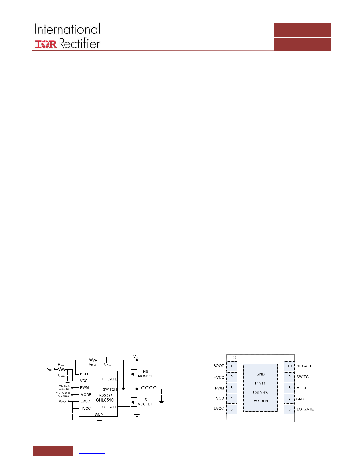
BASIC APPLICATION
PIN DIAGRAM
Figure 1: Basic Applications Circuit
1 www.irf.com | © 2014 International Rectifier
Figure 2: IR3537/CHL8510 Package Top View
January 9, 2015 | V1.2
1 page 
IR3537
12V High Performance Gate Driver CHL8510
ABSOLUTE MAXIMUM RATINGS
BOOT
+35.0V reference to GND,
+15V reference to SWITCH
PWM
+7.0V
VCC, HVCC
+15.0V
LVCC
LO_GATE
GND
SWITCH
HI_GATE
VCC+0.7Vdc to a maximum of +15.0V
DC: ‐0.3V to <0.3V above Vcc,
<200ns: ‐2V to <0.3V above Vcc
0V+/‐ 0V
DC: ‐0.3V to +15V, <20nS: 25V, <5nS: ‐10V,
<20 ns: ‐4Vdc and <200 ns: ‐2Vdc
DC: SWITCH – 0.3V to 0.3V above VBOOT,
<200ns: SWITCH – 2V to 0.3V above VBOOT
MODE
‐0.3V to +15.0V
ESD – Charged Device Model JESD22‐C101‐C
Passes +/‐1000V
THERMAL INFORMATION
Thermal Resistance (θJC)
Thermal Resistance (θJA)1
Maximum Operating Junction Temperature
3°C/W
45°C/W
150°C
Maximum Storage Temperature Range
‐65°C to 150°C
Maximum Lead Temperature (Soldering 10s)
300°C
Note 1: θJA is measured with the component mounted on a high effective thermal conductivity test board in free air.
Stresses beyond those listed under “Absolute Maximum Ratings” may cause permanent damage to the device. These are stress ratings
only and functional operation of the device at these or any other conditions beyond those indicated in the operational sections of the
specifications are not implied.
5 www.irf.com | © 2014 International Rectifier
January 9, 2015 | V1.2
5 Page 
IR3537
12V High Performance Gate Driver CHL8510
supply voltage plus the HVCC voltage less the diode
forward voltage.
When the PWM signal goes low, the MOSFET is turned off
by pulling the MOSFET gate to the SWITCH voltage.
LOW‐SIDE DRIVER
The IR3537/CHL8510 low‐side driver is designed to drive
an external N‐channel MOSFET referenced to ground at up
to 1MHz. The low‐side driver is connected internally to the
LVCC supply voltage.
ADAPTIVE DEAD TIME ADJUSTMENT
In a synchronous buck configuration, dead time between
the turn off of one gate and turn on of the other is
necessary to prevent simultaneous conduction of the
external MOSFETS preventing a shoot‐through condition
which would result in a short of the supply voltage to
ground. A fixed dead time does not provide optimal
performance across a variety of MOSFETs and board
layouts.
The IR3537/CHL8510 provides an ‘adaptive’ dead time
adjustment. This feature minimizes dead time which
maximizes efficiency. The ‘break before make’ adaptive
design is achieved by monitoring gate and SWITCH
voltages to determine OFF status of a MOSFET. It also
provides zero‐voltage switching (ZVS) of the low‐side
MOSFET with minimum current conduction through its
body‐diode.
INDEPENDENT VARIABLE GATE VOLTAGE
The IR3537/CHL8510 features independent variable
gate voltages for both the high‐ and low‐side drivers.
This enables implementation of the Variable Gate Drive
(VGD) feature in VR circuits using the IR multiphase
controllers to improve efficiency.
The voltage applied to the HVCC and LVCC pins of
IR3537/CHL8510 determines the gate voltage on the
external MOSFETs. These pins may be powered from
independent voltage sources or tied together to a common
voltage source. Variation in the gate voltage allows
efficiency to be optimized across the load current range by
trading off conduction and switching losses. Increasing the
voltage across a MOSFET gate, results in reduced Rdson
which lowers the MOSFET conduction losses, but also
raises the gate charge which increases the switching losses.
The voltage on each HVCC and LVCC pin, and thus the gate
drive voltage of the CHL8510, can be varied from 4.5V to
13.2V.
The International Rectifier’s digital multiphase controllers
provide a unique VAR_GATE output which varies inversely
with the VR output current. The VAR_GATE output is
designed to be used with an external circuit and provide
the optimum voltage across the IR3537/CHL8510’s HVCC
and LVCC pins for optimum system efficiency across the
load range.
When the PWM is switching between 1.8V and 0V, its
falling edge transition from high to low will turn off the
high‐side gate driver. The adaptive dead time circuit
monitors the HI_GATE and the SWITCH node voltages
during the high‐side MOSFET turn off. When the HI_GATE
falls below 1.7V above the SWITCH node potential or the
SWITCH node voltage drops below 0.8V, the high‐side
MOSFET is determined to be turned off, and the LO_GATE
turn‐on is initiated. This turns on the external low‐side
MOSFET. The rising edge transition of the PWM signal from
low to high voltage causes the low‐side gate driver to turn
off. The adaptive circuit monitors the voltage at LO_GATE
and when it falls below 1.7V, the low‐side MOSFET is
turned off, and the high‐side MOSFET turn‐on is initiated.
This turns on the external high‐side MOSFET.
11 www.irf.com | © 2014 International Rectifier
January 9, 2015 | V1.2
11 Page | ||
| Páginas | Total 15 Páginas | |
| PDF Descargar | [ Datasheet CHL8510.PDF ] | |
Hoja de datos destacado
| Número de pieza | Descripción | Fabricantes |
| CHL8510 | 12V High Performance Gate Driver | International Rectifier |
| CHL8510 | HIGH EFFICIENCY 6A BUCK MOSFET DRIVER | CHiL Semiconductor |
| Número de pieza | Descripción | Fabricantes |
| SLA6805M | High Voltage 3 phase Motor Driver IC. |
Sanken |
| SDC1742 | 12- and 14-Bit Hybrid Synchro / Resolver-to-Digital Converters. |
Analog Devices |
|
DataSheet.es es una pagina web que funciona como un repositorio de manuales o hoja de datos de muchos de los productos más populares, |
| DataSheet.es | 2020 | Privacy Policy | Contacto | Buscar |