|
|
|
PDF A1324 Data sheet ( Hoja de datos )
| Número de pieza | A1324 | |
| Descripción | Linear Hall Effect Sensor ICs | |
| Fabricantes | Allegro MicroSystems | |
| Logotipo | ||
Hay una vista previa y un enlace de descarga de A1324 (archivo pdf) en la parte inferior de esta página. Total 12 Páginas | ||
|
No Preview Available !
A1324, A1325, and A1326
Low Noise, Linear Hall Effect Sensor ICs with Analog Output
Features and Benefits
• Temperature-stable quiescent output voltage and sensitivity
• Output voltage proportional to magnetic flux density
• Low-noise output increases accuracy
• Precise recoverability after temperature cycling
• Ratiometric rail-to-rail output
• Wide ambient temperature range: –40°C to 150°C
• Immune to mechanical stress
• Solid-state reliability
• Enhanced EMC performance for stringent automotive
applications
Packages
3-pin ultramini SIP
1.5 mm × 4 mm × 3 mm
(suffix UA)
3-pin SOT23-W
2 mm × 3 mm × 1 mm
(suffix LH)
Approximate footprint
Description
New applications for linear output Hall-effect devices, such
as displacement, angular position, and current measurement,
require high accuracy in conjunction with small package size.
The Allegro™ A1324, A1325, and A1326 linear Hall-effect
sensor ICs are designed specifically to achieve both goals. This
temperature-stable device is available in a miniature surface
mount package (SOT23W) and an ultra-mini through-hole
single in-line package.
These ratiometric Hall effect sensor ICs provide a voltage
output that is proportional to the applied magnetic field. They
feature a quiescent voltage output of 50% of the supply voltage.
The A1324/25/26 feature factory programmed sensitivities of
5.0 mV/G, 3.125 mV/G, and 2.5 mV/G, respectively.
The features of these linear devices make them ideal for
use in automotive and industrial applications requiring high
accuracy, and operate through an extended temperature range,
–40°C to 150°C.
Each BiCMOS monolithic circuit integrates a Hall element,
temperature-compensating circuitry to reduce the intrinsic
sensitivity drift of the Hall element, a small-signal high-gain
amplifier, a clamped low-impedance output stage, and a
proprietary dynamic offset cancellation technique.
These devices are available in a 3-pin ultra-mini SIP package
(UA), and a 3-pin surface mount SOT-23 style package (LH). Both
are lead (Pb) free, with 100% matte tin leadframe plating.
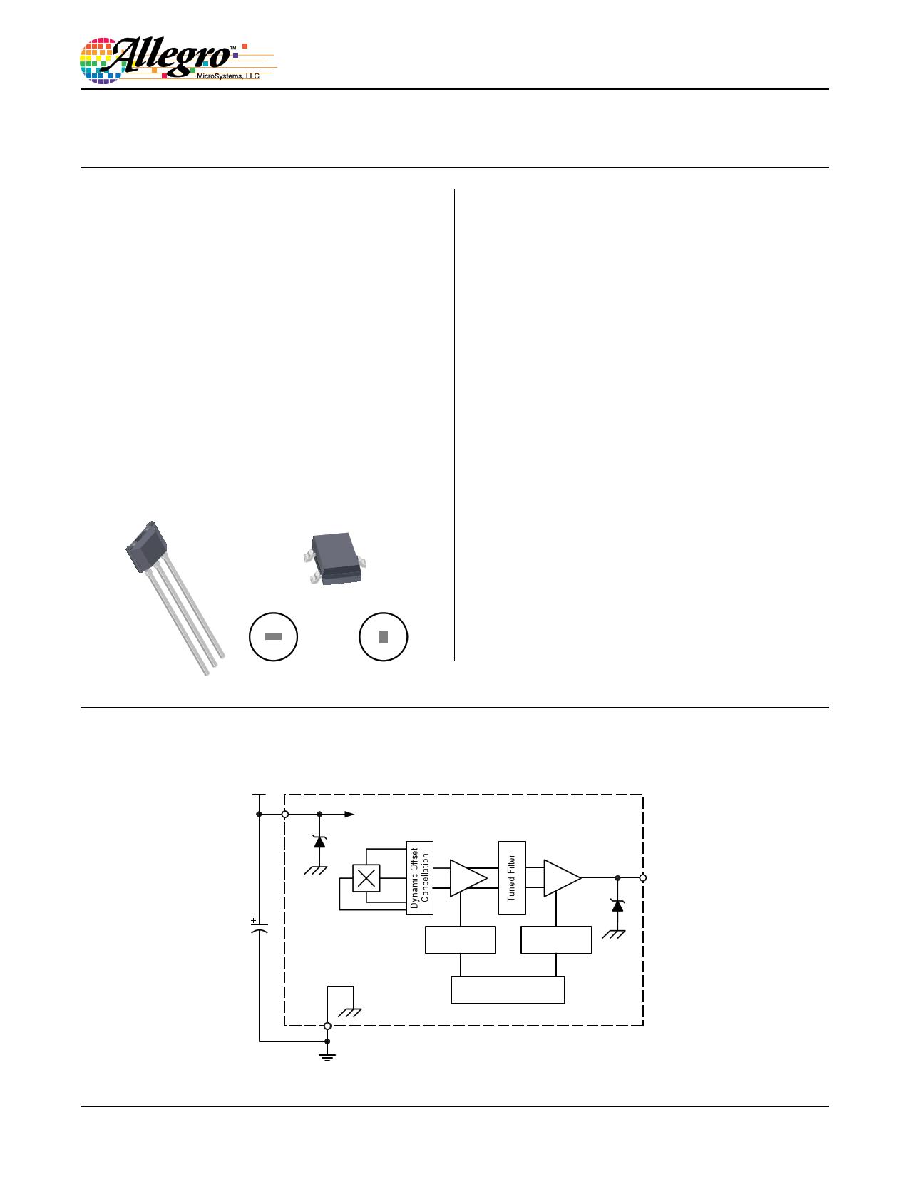
V+
VCC
Functional Block Diagram
To All Subcircuits
GND
Sensitivity and
Sensitivity TC
Offset
Trim Control
VOUT
A1324-DS, Rev. 4
1 page 
A1324, A1325,
and A1326
Linear Hall Effect Sensor ICs with Analog Output
Characteristic Definitions
Power-On Time When the supply is ramped to its operating
voltage, the device output requires a finite time to react to an
input magnetic field. Power-On Time is defined as the time it
takes for the output voltage to begin responding to an applied
magnetic field after the power supply has reached its minimum
specified operating voltage, VCC(min).
V
VCC(typ.)
90% VOUT
VCC
VOUT
VCC(min.)
tPO
t1 t2
t1=
time at which power supply reaches
minimum specified operating voltage
t2=
time at which output voltage settles
within ±10% of its steady state value
under an applied magnetic field
0 +t
Quiescent Voltage Output In the quiescent state (that is, with
no significant magnetic field: B = 0), the output, VOUT(Q) , equals
a ratio of the supply voltage, VCC , throughout the entire operat-
ing range of VCC and the ambient temperature, TA .
Quiescent Voltage Output Drift Through Temperature
Range Due to internal component tolerances and thermal con-
siderations, the quiescent voltage output, VOUT(Q) , may drift from
its nominal value through the operating ambient temperature
range, TA . For purposes of specification, the Quiescent Voltage
Output Drift Through Temperature Range, ∆VOUT(Q) (mV), is
defined as:
∆VOUT(Q) = VOUT(Q)TA – VOUT(Q)25°C
(1)
Sensitivity The presence of a south-polarity magnetic field
perpendicular to the branded surface of the package increases the
output voltage from its quiescent value toward the supply voltage
rail. The amount of the output voltage increase is proportional
to the magnitude of the magnetic field applied. Conversely, the
application of a north polarity field will decrease the output volt-
age from its quiescent value. This proportionality is specified
as the magnetic sensitivity, Sens (mV/G), of the device and is
defined as:
Sens
=
VOUT(B+) – VOUT(B–)
B(+) – B(–)
(2)
where B(+) and B(–) are two magnetic fields with opposite
polarities.
Sensitivity Temperature Coefficient The device sensitivity
changes with temperature, with respect to its sensitivity tem-
perature coefficient, TCSENS . TCSENS is programmed at 150°C,
and calculated relative to the nominal sensitivity programming
temperature of 25°C. TCSENS (%/°C) is defined as:
TCSens
=
SensSTe2n–sTS1ensT1
×
100%
T21–T1
(3)
where T1 is the nominal Sens programming temperature of 25°C,
and T2 is the TCSENS programming temperature of 150°C.
The ideal value of sensitivity through the temperature range,
SensIDEAL(TA), is defined as:
SensIDEAL(TA) = SensT1 × (100% + TCSENS(TA –T1) ) (4)
Sensitivity Drift Through Temperature Range Second
order sensitivity temperature coefficient effects cause the mag-
netic sensitivity to drift from its ideal value through the operating
ambient temperature, TA. For purposes of specification, the sensi-
tivity drift through temperature range, ∆SensTC , is defined as:
∆SensTC =
SensTA – SensIDEAL(TA)
SensIDEAL(TA)
×
100%
(5)
Sensitivity Drift Due to Package Hysteresis Package
stress and relaxation can cause the device sensitivity at TA = 25°C
to change during or after temperature cycling. This change in
sensitivity follows a hysteresis curve.
For purposes of specification, the Sensitivity Drift Due to Pack-
age Hysteresis, ∆SensPKG , is defined as:
∆SensPKG =
Sens(25°C)2 – Sens(25°C)1
Sens(25°C)1
×100%
(6)
where Sens(25°C)1 is the programmed value of sensitivity at
Allegro MicroSystems, LLC
115 Northeast Cutoff
Worcester, Massachusetts 01615-0036 U.S.A.
1.508.853.5000; www.allegromicro.com
5
5 Page 
A1324, A1325,
and A1326
Linear Hall Effect Sensor ICs with Analog Output
Package UA, 3-Pin SIP
4.09
+0.08
–0.05
45°
B
E 2.05 NOM
3.02
+0.08
–0.05
1.44 NOM
E
1.02
MAX
12 3
10°
E
Branded
Face
0.79 REF
A
14.99 ±0.25
0.43
+0.05
–0.07
1.27 NOM
C
1.52 ±0.05
Mold Ejector
Pin Indent
45°
NNN
1
D Standard Branding Reference View
= Supplier emblem
N = Last three digits of device part number
0.41
+0.03
–0.06
For Reference Only; not for tooling use (reference DWG-9065)
Dimensions in millimeters
Dimensions exclusive of mold flash, gate burrs, and dambar protrusions
Exact case and lead configuration at supplier discretion within limits shown
A Dambar removal protrusion (6X)
B Gate and tie bar burr area
C Active Area Depth, 0.50 mm REF
D Branding scale and appearance at supplier discretion
E Hall element (not to scale)
Allegro MicroSystems, LLC
115 Northeast Cutoff
Worcester, Massachusetts 01615-0036 U.S.A.
1.508.853.5000; www.allegromicro.com
11
11 Page | ||
| Páginas | Total 12 Páginas | |
| PDF Descargar | [ Datasheet A1324.PDF ] | |
Hoja de datos destacado
| Número de pieza | Descripción | Fabricantes |
| A1320 | PNP Transistor - 2SA1320 | Toshiba Semiconductor |
| A132000 | ADPCM SOUND CONTROLLER | AMIC Technology |
| A132000H | ADPCM SOUND CONTROLLER | AMIC Technology |
| A1321 | Ratiometric Linear Hall Effect Sensor for High-Temperature Operation | Allegro MicroSystems |
| Número de pieza | Descripción | Fabricantes |
| SLA6805M | High Voltage 3 phase Motor Driver IC. |
Sanken |
| SDC1742 | 12- and 14-Bit Hybrid Synchro / Resolver-to-Digital Converters. |
Analog Devices |
|
DataSheet.es es una pagina web que funciona como un repositorio de manuales o hoja de datos de muchos de los productos más populares, |
| DataSheet.es | 2020 | Privacy Policy | Contacto | Buscar |