|
|
|
PDF ACPL-C87A Data sheet ( Hoja de datos )
| Número de pieza | ACPL-C87A | |
| Descripción | Precision Optically Isolated Voltage Sensor | |
| Fabricantes | AVAGO | |
| Logotipo | ||
Hay una vista previa y un enlace de descarga de ACPL-C87A (archivo pdf) en la parte inferior de esta página. Total 14 Páginas | ||
|
No Preview Available !
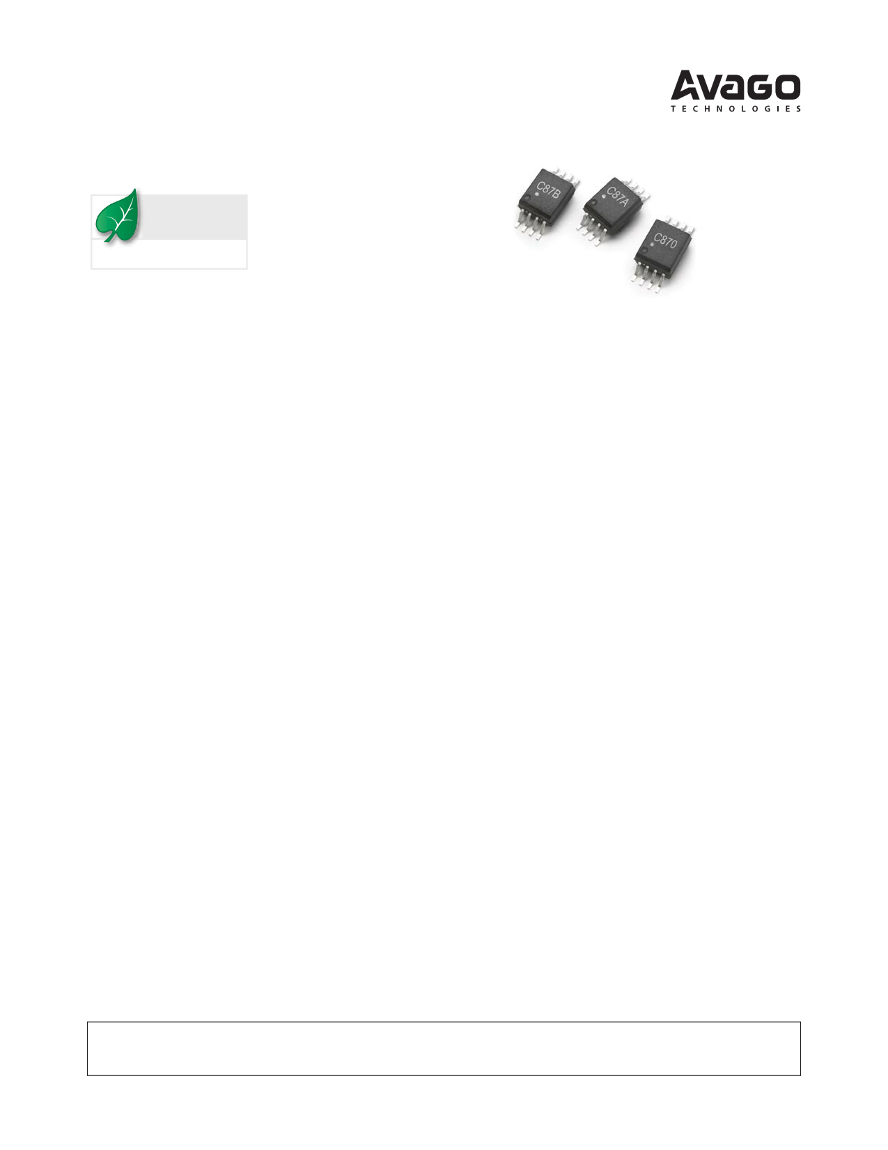
ACPL-C87B, ACPL-C87A, ACPL-C870
Precision Optically Isolated Voltage Sensor
Data Sheet
Lead (Pb) Free
RoHS 6 fully
compliant
RoHS 6 fully compliant options available;
-xxxE denotes a lead-free product
Description
The ACPL-C87B/C87A/C870 voltage sensors are optical
isolation amplifiers designed specifically for voltage
sensing. Its 2 V input range and high 1 G input impe-
dance, makes it well suited for isolated voltage sensing
requirements in electronic power converters applications
including motor drives and renewable energy systems.
In a typical voltage sensing implementation, a resistive
voltage divider is used to scale the DC-link voltage to suit
the input range of the voltage sensor. A differential output
voltage that is proportional to the input voltage is created
on the other side of the optical isolation barrier.
For general applications, the ACPL-C87A (±1% gain
tolerance) and the ACPL-C870 (±3% gain tolerance)
are recommended. For high precision requirements,
the ACPL-C87B (±0.5% gain tolerance) can be used. The
ACPL-C87B/C87A/C870 family operates from a single 5 V
supply and provides excellent linearity. An active-high
shutdown pin is available which reduces the IDD1 current
to only 15 A, making them suitable for battery-powered
and other power-sensitive applications.
The high common-mode transient immunity (15 kV/s)
of the ACPL-C87B/C87A/C870 provides the precision and
stability needed to accurately monitor DC-link voltage in
high noise environments. Combined with superior optical
coupling technology, the ACPL-C87B/C87A/C870 imple-
ments sigma-delta (-) modulation, chopper stabilized
amplifiers, and differential outputs to provide unequaled
isolation-mode noise rejection, low offset, high gain
accuracy and stability. This performance is delivered in a
compact, auto-insertable Stretched SO-8 (SSO-8) package
that meets worldwide regulatory safety standards.
Features
Advanced Sigma-Delta (-) Modulation Technology
Unity Gain 1V/V, ±0.5% High Gain Accuracy (ACPL-C87B)
1 G Input Impedence
0 to 2 V Nominal Input Range
-35 ppm/°C Low Gain Drift
21V /°C Offset Voltage Drift
0.1% Non-Linearity Max
Active-High Shutdown Pin
100 kHz Wide Bandwidth
3 V to 5.5 V Wide Supply Range for Output Side
-40° C to +105° C Operating Temperature Range
15 kV/s Common-Mode Transient Immunity
Compact, Auto-Insertable Stretched SO-8 Package
Safety and Regulatory Approvals (pending):
– IEC/EN/DIN EN 60747-5-5: 1230 Vpeak working
insulation voltage
– UL 1577: 5000 Vrms/1 min double protection rating
– CSA: Component Acceptance Notice #5
Applications
Isolated Voltage Sensing in AC and Servo Motor Drives
Isolated DC-Bus Voltage Sensing in Solar Inverters,
Wind Turbine Inverters
Isolated Sensor Interfaces
Signal Isolation in Data Acquisition Systems
General Purpose Voltage Isolation
CAUTION: It is advised that normal static precautions be taken in handling and assembly
of this component to prevent damage and/or degradation which may be induced by ESD.
1 page 
Table 5. Absolute Maximum Rating
Parameter
Symbol
Min. Max.
Storage Temperature
Ambient Operating Temperature
Supply Voltage
Steady-State Input Voltage [1, 3]
Two-Second Transient Input Voltage [2]
Logic Input
Output Voltages
Lead Solder Temperature
TS -55 +125
TA -40 +105
VDD1, VDD2
-0.5 6.0
VIN -2 VDD1 + 0.5
VIN -6 VDD1 + 0.5
VSD -0.5 VDD1 + 0.5
VOUT+, VOUT− -0.5 VDD2 + 0.5
260° C for 10 sec., 1.6 mm below seating plane
Notes:
1. DC voltage of up to -2 V on the inputs does not cause latch-up or damage to the device.
2. Transient voltage of 2 seconds up to -6 V on the inputs does not cause latch-up or damage to the device.
3. Absolute maximum DC current on the inputs = 100 mA, no latch-up or device damage occurs.
Units
°C
°C
V
V
V
V
V
Table 6. Recommended Operating Conditions
Parameter
Symbol
Ambient Operating Temperature
TA
VDD1 Supply Voltage
VDD1
VDD2 Supply Voltage
VDD2
Input Voltage Range[1]
VIN
Shutdown Enable Voltage
VSD
Notes:
1. 2 V is the nominal input range. Full scale input range (FSR) is 2.46 V.
Min.
-40
4.5
3.0
0
VDD1 – 0.5
Max.
+105
5.5
5.5
2.0
VDD1
Units
°C
V
V
V
V
5
5 Page 
Definitions
Gain
Gain is defined as the slope of the best-fit line of differen-
tial output voltage (VOUT+ – VOUT-) over the nominal input
range, with offset error adjusted out.
Nonlinearity
Nonlinearity is defined as half of the peak-to-peak output
deviation from the best-fit gain line, expressed as a per-
centage of the full-scale differential output voltage.
Common Mode Transient Immunity, CMTI, also known
as Common Mode Rejection
CMTI is tested by applying an exponentially rising/falling
voltage step on pin 4 (GND1) with respect to pin 5 (GND2).
The rise time of the test waveform is set to approximately
50 ns. The amplitude of the step is adjusted until the dif-
ferential output (VOUT+ – VOUT-) exhibits more than a 200
mV deviation from the average output voltage for more
than 1μs. The ACPL-C87x will continue to function if more
than 10 kV/s common mode slopes are applied, as long
as the breakdown voltage limitations are observed.
Power Supply Rejection, PSR
PSRR is the ratio of differential amplitude of the ripple
outputs over power supply ripple voltage, referred to the
input, expressed in dB.
Application Information
Application Circuit
The typical application circuit is shown in Figure 19.
The ACPL-C87X voltage sensor is often used in photo-
voltaic (PV) panel voltage measurement and tracking in
PV inverters, and DC bus voltage monitoring in motor
drivers. The high voltage across rails needs to be scaled
down to fit the input range of the iso-amp by choosing R1
and R2 values according to appropriate ratio.
The ACPL-C87X senses the single-ended input signal
and produces differential outputs across the galvanic
isolation barrier. The differential outputs (Vout+, Vout-)
can be connected to an op-amp to convert to a single-
ended signal or directly to two ADCs. The op-amp used in
the external post-amplifier circuit should be of sufficiently
high precision so that it does not contribute a significant
amount of offset or offset drift relative to the contribu-
tion from the isolation amplifier. Generally, op-amps with
bipolar input stages exhibit better offset performance
than op-amps with JFET or MOSFET input stages.
In addition, the op-amp should also have enough
bandwidth and slew rate so that it does not adversely
affect the response speed of the overall circuit. The post-
amplifier circuit includes a pair of capacitors (C4 and C5)
that form a single-pole low-pass filter; these capacitors
allow the bandwidth of the post-amp to be adjusted in-
dependently of the gain and are useful for reducing the
output noise from the isolation amplifier.
The gain-setting resistors in the post-amp should have a
tolerance of 1% or better to ensure adequate CMRR and
adequate gain tolerance for the overall circuit. Resistor
networks can be used that have much better ratio toler-
ances than can be achieved using discrete resistors. A
resistor network also reduces the total number of compo-
nents for the circuit as well as the required board space.
C5
100 pF
L1
R1
R2
10K
L2
VDD1
C1 C2
100 pF 100 nF
U1
1 VDD1
VDD2 8
2 VIN
VOUT+ 7
ACPL-C87X
3 SHDN
VOUT- 6
VDD2
C3
100 nF
4 GND1
GND2 5
GND1 GND2
R3
10K,1%
R4
10K,1%
R6
10K, 1%
C4
100 pF
R5
10K, 1%
V+
Vout
U2
OPA237
V-
Figure 19. Typical application circuit.
GND2
11
11 Page | ||
| Páginas | Total 14 Páginas | |
| PDF Descargar | [ Datasheet ACPL-C87A.PDF ] | |
Hoja de datos destacado
| Número de pieza | Descripción | Fabricantes |
| ACPL-C870 | Precision Optically Isolated Voltage Sensor | AVAGO |
| ACPL-C87A | Precision Optically Isolated Voltage Sensor | AVAGO |
| ACPL-C87B | Precision Optically Isolated Voltage Sensor | AVAGO |
| Número de pieza | Descripción | Fabricantes |
| SLA6805M | High Voltage 3 phase Motor Driver IC. |
Sanken |
| SDC1742 | 12- and 14-Bit Hybrid Synchro / Resolver-to-Digital Converters. |
Analog Devices |
|
DataSheet.es es una pagina web que funciona como un repositorio de manuales o hoja de datos de muchos de los productos más populares, |
| DataSheet.es | 2020 | Privacy Policy | Contacto | Buscar |