|
|
|
PDF ADP221 Data sheet ( Hoja de datos )
| Número de pieza | ADP221 | |
| Descripción | High PSRR Voltage Regulator | |
| Fabricantes | Analog Devices | |
| Logotipo | ||
Hay una vista previa y un enlace de descarga de ADP221 (archivo pdf) en la parte inferior de esta página. Total 20 Páginas | ||
|
No Preview Available !
Data Sheet
FEATURES
Input voltage range: 2.5 V to 5.5 V
Dual independent 200 mA low dropout voltage regulators
Miniature 6-ball, 1.0 mm × 1.5 mm WLCSP and 6-ball
bumped bare die
Initial accuracy: ±1%
Stable with 1 µF ceramic output capacitors
No noise bypass capacitor required
Two independent logic controlled enables
Overcurrent and thermal protection
Active output pull-down (ADP221)
Key specifications
High PSRR
76 dB PSRR up to 1 kHz
70 dB PSRR at 10 kHz
60 dB PSRR at 100 kHz
40 dB PSRR at 1 MHz
Low output noise
27 µV rms typical output noise at VOUT = 1.2 V
50 µV rms typical output noise at VOUT = 2.8 V
Excellent transient response
Low dropout voltage: 150 mV @ 200 mA load
60 µA typical ground current at no load, both LDOs enabled
100 µs fast turn-on circuit
Guaranteed 200 mA output current per regulator
−40°C to +125°C junction temperature
APPLICATIONS
Mobile phones
Digital cameras and audio devices
Portable and battery-powered equipment
Portable medical devices
Post dc-to-dc regulation
GENERAL DESCRIPTION
The 200 mA dual output ADP220/ADP221 combine high PSRR,
low noise, low quiescent current, and low dropout voltage in a
voltage regulator ideally suited for wireless applications with
demanding performance and board space requirements.
The low quiescent current, low dropout voltage, and wide input
voltage range of the ADP220/ADP221 extend the battery life of
portable devices. The ADP220/ADP221 maintain power supply
rejection greater than 60 dB for frequencies as high as 100 kHz
while operating with a low headroom voltage. The ADP220
offers much lower noise performance than competing LDOs
Dual, 200 mA, Low Noise,
High PSRR Voltage Regulator
ADP220/ADP221
TYPICAL APPLICATION CIRCUITS
12
ON
OFF
A
EN1
VOUT1
VOUT1 = 2.8V
1µF
B
ON
OFF
C
GND
VIN
TOP VIEW
(Not to Scale)
EN2 VOUT2
VIN = 3.3V
1µF
VOUT2 = 2.8V
1µF
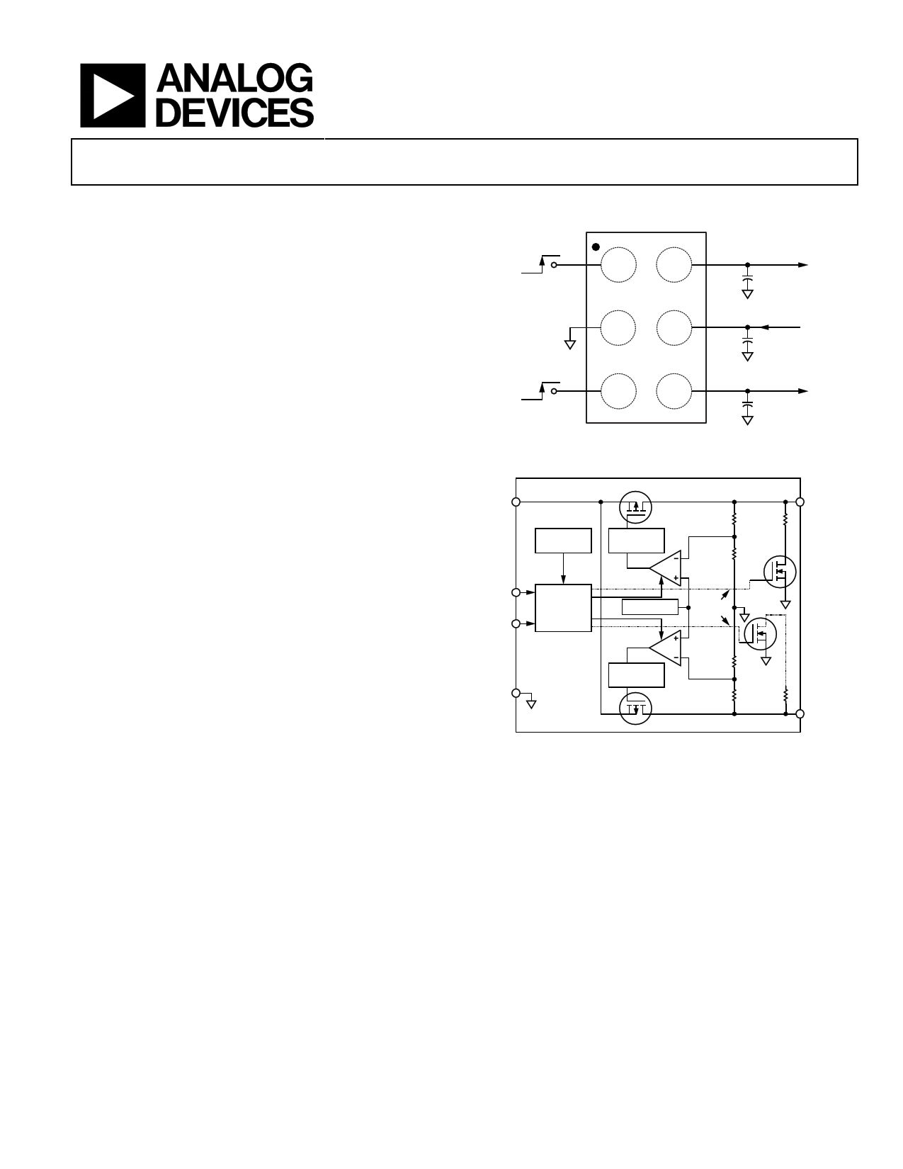
Figure 1. Typical Application Circuit
VIN
THERMAL
SHUTDOWN
CURRENT
LIMIT
VOUT1
60Ω
EN1 CONTROL
LOGIC
AND
EN2 ENABLE
REFERENCE
ADP221
ONLY
ADP220
GND
CURRENT
LIMIT
60Ω
VOUT2
Figure 2. Block Diagram of the ADP220/ADP221
without the need for a noise bypass capacitor. The ADP221 also
includes an active pull-down to quickly discharge output loads.
The ADP220/ADP221 are available in a miniature 6-ball
WLCSP package and 6-ball bumped bare die and is stable with
tiny 1 µF ± 30% ceramic output capacitors, resulting in the smallest
possible board area for a wide variety of portable power needs.
The ADP220/ADP221 are available in many output voltage
combinations, ranging from 0.8 V to 3.3 V, and offer overcur-
rent and thermal protection to prevent damage in adverse
conditions.
Rev. H
Document Feedback
Information furnished by Analog Devices is believed to be accurate and reliable. However, no
responsibilityisassumedbyAnalogDevices for itsuse,nor foranyinfringementsofpatentsor other
rights of third parties that may result from its use. Specifications subject to change without notice. No
license is granted by implication or otherwise under any patent or patent rights of Analog Devices.
Trademarksandregisteredtrademarksarethepropertyoftheirrespectiveowners.
One Technology Way, P.O. Box 9106, Norwood, MA 02062-9106, U.S.A.
Tel: 781.329.4700 ©2008–2013 Analog Devices, Inc. All rights reserved.
Technical Support
www.analog.com
1 page 
Data Sheet
ABSOLUTE MAXIMUM RATINGS
Table 3.
Parameter
VIN to GND
VOUT1, VOUT2 to GND
EN1, EN2 to GND
Storage Temperature Range
Operating Junction Temperature Range
Soldering Conditions
Rating
–0.3 V to +6.5 V
–0.3 V to VIN
–0.3 V to +6.5 V
–65°C to +150°C
–40°C to +125°C
JEDEC J-STD-020
Stresses above those listed under Absolute Maximum Ratings
may cause permanent damage to the device. This is a stress
rating only; functional operation of the device at these or any
other conditions above those indicated in the operational
section of this specification is not implied. Exposure to absolute
maximum rating conditions for extended periods may affect
device reliability.
THERMAL DATA
Absolute maximum ratings apply individually only, not in
combination.
The ADP220/ADP221 can be damaged when the junction
temperature limits are exceeded. Monitoring ambient temper-
ature does not guarantee that the junction temperature (TJ)
is within the specified temperature limits. In applications
with high power dissipation and poor thermal resistance, the
maximum ambient temperature may have to be derated. In
applications with moderate power dissipation and low PCB
thermal resistance, the maximum ambient temperature can
exceed the maximum limit as long as the junction temperature
is within specification limits. The junction temperature (TJ) of
the device is dependent on the ambient temperature (TA), the
power dissipation of the device (PD), and the junction-to-ambient
thermal resistance of the package (θJA). Maximum junction
temperature (TJ) is calculated from the ambient temperature
(TA) and power dissipation (PD) using the following formula:
TJ = TA + (PD × θJA)
ADP220/ADP221
Junction-to-ambient thermal resistance (θJA) of the package is
based on modeling and calculation using a 4-layer board. The
junction-to-ambient thermal resistance is highly dependent
on the application and board layout. In applications where high
maximum power dissipation exists, close attention to thermal
board design is required. The value of θJA may vary, depending
on PCB material, layout, and environmental conditions. The
specified values of θJA are based on a four-layer, 4 inch × 3 inch,
circuit board. Refer to JEDEC JESD 51-9 for detailed informa-
tion on the board construction. For additional information,
see the AN-617 Application Note, MicroCSPTM Wafer Level Chip
Scale Package.
ΨJB is the junction-to-board thermal characterization parameter
with units of °C/W. ΨJB of the package is based on modeling and
calculation using a 4-layer board. The JESD51-12, Guidelines
for Reporting and Using Package Thermal Information, states
that thermal characterization parameters are not the same as
thermal resistances. ΨJB measures the component power flowing
through multiple thermal paths rather than a single path as in
thermal resistance, θJB. Therefore, ΨJB thermal paths include
convection from the top of the package as well as radiation
from the package. Factors that make ΨJB more useful in real-
world applications. Maximum junction temperature (TJ) is
calculated from the board temperature (TB) and power
dissipation (PD) using the following formula:
TJ = TB + (PD × ΨJB)
Refer to JEDEC JESD51-8 and JESD51-12 for more detailed
information on ΨJB.
THERMAL RESISTANCE
θJA and ΨJB are specified for the worst-case conditions, that is, a
device soldered in a circuit board for surface-mount packages.
Table 4.
Package Type
6-Ball, 0.5 mm Pitch WLCSP
6-Ball Bumped Bare Die
θJA ΨJB Unit
260 43.8 °C/W
260 43.8 °C/W
ESD CAUTION
Rev. H | Page 5 of 20
5 Page 
Data Sheet
THEORY OF OPERATION
The ADP220/ADP221 are low quiescent current, low dropout
linear regulators that operate from 2.5 V to 5.5 V and provide
up to 200 mA of current from each output. Drawing a low 120 μA
quiescent current (typical) at full load makes the ADP220/
ADP221 ideal for battery-operated portable equipment. Shut-
down current consumption is typically 100 nA.
Optimized for use with small 1 µF ceramic capacitors, the
ADP220/ADP221 provide excellent transient performance.
VIN
THERMAL
SHUTDOWN
CURRENT
LIMIT
VOUT1
60Ω
EN1 CONTROL
LOGIC
AND
EN2 ENABLE
REFERENCE
ADP221
ONLY
ADP220
GND
CURRENT
LIMIT
60Ω
VOUT2
Figure 28. Internal Block Diagram
ADP220/ADP221
Internally, the ADP220/ADP221 consist of a reference, two error
amplifiers, two feedback voltage dividers, and two PMOS pass
transistors. Output current is delivered via the PMOS pass device,
which is controlled by the error amplifier. The error amplifier
compares the reference voltage with the feedback voltage from
the output and amplifies the difference. If the feedback voltage
is lower than the reference voltage, the gate of the PMOS device
is pulled lower, allowing more current to flow and increasing
the output voltage. If the feedback voltage is higher than the
reference voltage, the gate of the PMOS device is pulled higher,
allowing less current to flow and decreasing the output voltage.
The ADP221 also includes an active pull-down circuit to rapidly
discharge the output load capacitance when each output is
disabled.
The ADP220/ADP221 are available in multiple output voltage
options ranging from 0.8 V to 3.3 V. The ADP220/ADP221 use
the EN1/EN2 pins to enable and disable the VOUT1/VOUT2
pins under normal operating conditions. When EN1/EN2 are high,
VOUT1/VOUT2 turn on; when EN1/EN2 are low, VOUT1/
VOUT2 turn off. For automatic startup, EN1/EN2 can be tied
to VIN.
Rev. H | Page 11 of 20
11 Page | ||
| Páginas | Total 20 Páginas | |
| PDF Descargar | [ Datasheet ADP221.PDF ] | |
Hoja de datos destacado
| Número de pieza | Descripción | Fabricantes |
| ADP220 | High PSRR Voltage Regulator | Analog Devices |
| ADP221 | High PSRR Voltage Regulator | Analog Devices |
| ADP222 | High PSRR Voltage Regulators | Analog Devices |
| ADP223 | High PSRR Voltage Regulators | Analog Devices |
| Número de pieza | Descripción | Fabricantes |
| SLA6805M | High Voltage 3 phase Motor Driver IC. |
Sanken |
| SDC1742 | 12- and 14-Bit Hybrid Synchro / Resolver-to-Digital Converters. |
Analog Devices |
|
DataSheet.es es una pagina web que funciona como un repositorio de manuales o hoja de datos de muchos de los productos más populares, |
| DataSheet.es | 2020 | Privacy Policy | Contacto | Buscar |