|
|
|
PDF GD25Q16 Data sheet ( Hoja de datos )
| Número de pieza | GD25Q16 | |
| Descripción | 16Mbit Dual and Quad SPI Flash | |
| Fabricantes | GigaDevice | |
| Logotipo | ||
1. GD25Q16 pdf datasheet Hay una vista previa y un enlace de descarga de GD25Q16 (archivo pdf) en la parte inferior de esta página. Total 30 Páginas | ||
|
No Preview Available !
Uniform Sector
16Mbit Dual and Quad SPI Flash
GD25Q16
FEATURES
◆ 16M-bit Serial Flash
-2048K-byte
-256 bytes per programmable page
◆ Standard, Dual, Quad SPI
-Standard SPI: SCLK, CS#, SI, SO, WP#, HOLD#
-Dual SPI: SCLK, CS#, IO0, IO1, WP#, HOLD#
-Quad SPI: SCLK, CS#, IO0, IO1, IO2, IO3
◆ High Speed Clock Frequency
-120MHz for fast read with 30PF load
-Dual I/O Data transfer up to 180Mbits/s
-Quad I/O Data transfer up to 360Mbits/s
◆ Program/Erase Speed
-Page Program time: 0.7ms typical
-Sector Erase time: 50ms typical
-Block Erase time: 0.2/0.28/0.6s typical
-Chip Erase time: 10s typical
◆ Flexible Architecture
-Sector of 4K-byte
-Block of 32/64/128K-byte
◆ Low Power Consumption
-20mA maximum active current
-5uA maximum power down current
◆ Software/Hardware Write Protection
-Write protect all/portion of memory via software
-Enable/Disable protection with WP# Pin
-Top or Bottom, Sector or Block selection
◆ Single Power Supply Voltage
-Full voltage range:2.7~3.6V
◆ Minimum 100,000 Program/Erase Cycles
GENERAL DESCRIPTION
The GD25Q16 (16M-bit) SPI flash supports the standard Serial Peripheral Interface (SPI), and supports the
Dual/Quad SPI: Serial Clock, Chip Select, Serial Data I/O0 (SI), I/O1 (SO), I/O2 (WP#), and I/O3 (HOLD#). The Dual I/O
data is transferred with speed of 180Mbits/s and the Quad I/O & Quad output data is transferred with speed of
360Mbits/s.
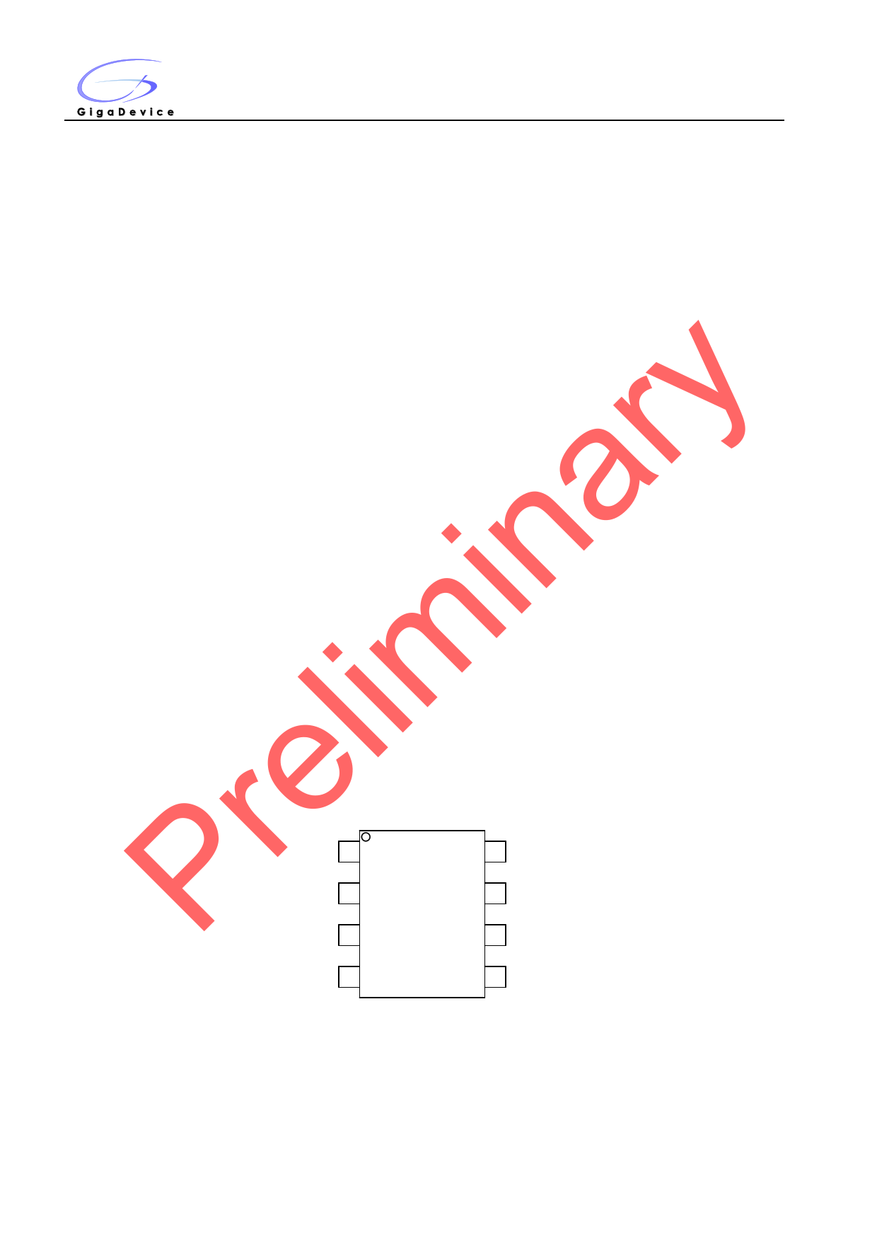
CONNECTION DIAGRAM
CS# 1
8
SO
WP#
27
Top View
36
VSS
45
8–LEAD SOP/DIP
VCC
HOLD#
SCLK
SI
1
1 page 
Uniform Sector
16Mbit Dual and Quad SPI Flash
GD25Q16
Data Protection
The GD25Q16 provide the following data protection methods:
◆ Write Enable (WREN) command: The WREN command is set the Write Enable Latch bit (WEL). The WEL bit will
return to reset by the following situation:
-Power-Up
-Write Disable (WRDI)
-Write Status Register (WRSR)
-Page Program (PP)
-Sector Erase (SE)
-Block Erase (BE)
-Chip Erase (CE)
◆ Software Protection Mode: The Block Protect (BP4, BP3, BP2, BP1, BP0) bits define the section of the memory
array that can be read but not change.
◆ Hardware Protection Mode: WP# going low to protected the BP0~BP4 bits and SRP0~1 bits.
◆ Deep Power-Down Mode: In Deep Power-Down Mode, all commands are ignored except the Release from Deep
Power-Down Mode command.
Table1. GD25Q16 Protected area size
Status Register Content
Memory Content
BP4 BP3 BP2 BP1 BP0
XX0 0 0
00001
00010
00011
00100
00101
Blocks
NONE
31
30 to 31
28 to 31
24 to 31
16 to 31
Addresses
NONE
1F0000H-1FFFFFH
1E0000H-1FFFFFH
1C0000H-1FFFFFH
180000H-1FFFFFH
100000H-1FFFFFH
Density
NONE
64KB
128KB
256KB
512KB
1M
Portion
NONE
Upper 1/32
Upper 1/16
Upper 1/8
Upper 1/4
Upper 1/2
01001
0
01010
0 to 1
01011
0 to 3
01100
0 to 7
0 1 1 0 1 0 to 15
X X 1 1 X 0 to 31
000000H-00FFFFH
000000H-01FFFFH
000000H-03FFFFH
000000H-07FFFFH
000000H-0FFFFFH
000000H-1FFFFFH
64KB
128KB
256KB
512KB
1M
2M
Lower 1/32
Lower 1/16
Lower 1/8
Lower 1/4
Lower 1/2
ALL
10001
10010
10011
1010X
31
31
31
31
1FF000H-1FFFFFH
1FE000H-1FFFFFH
1FC000H-1FFFFFH
1F8000H-1FFFFFH
4KB
8KB
16KB
32KB
Top Block
Top Block
Top Block
Top Block
11001
11010
11011
1110X
0
0
0
0
000000H-000FFFH
000000H-001FFFH
000000H-003FFFH
000000H-007FFFH
4KB
8KB
16KB
32KB
Bottom Block
Bottom Block
Bottom Block
Bottom Block
5
5 Page 
Uniform Sector
16Mbit Dual and Quad SPI Flash
GD25Q16
Read Data Bytes at Higher Speed (Fast Read) (0BH)
The Read Data Bytes at Higher Speed (Fast Read) command is for quickly reading data out. It is followed by a 3-byte
address (A23-A0) and a dummy byte, each bit being latched-in during the rising edge of SCLK. Then the memory content,
at that address, is shifted out on SO, each bit being shifted out, at a Max frequency fC, during the falling edge of SCLK. The
first byte addressed can be at any location. The address is automatically incremented to the next higher address after each
byte of data is shifted out.
Figure7. Read Data Bytes at Higher Speed Sequence Diagram
CS#
SCLK
0 1 2 3 4 5 6 7 8 9 10
28 29 30 31
SI
SO
CS#
SCLK
SI
SO
Command
0B
High-Z
24-bit address
23 22 21
3210
32 33 34 35 36 37 38 39 40 41 42 43 44 45 46 47
Dummy Byte
76543210
Data Out1
Data Out2
76543210765
MSB
MSB
Dual Output Fast Read (3BH)
The Dual Output Fast Read command is followed by 3-byte address (A23-A0) and a dummy byte, each bit being
latched in during the rising edge of SCLK, then the memory contents are shifted out 2-bit per clock cycle from SI and SO.
The command sequence is shown in followed Figure8. The first byte addressed can be at any location. The address is
automatically incremented to the next higher address after each byte of data is shifted out.
Figure8. Dual Output Fast Read Sequence Diagram
CS#
SCLK
0 1 2 3 4 5 6 7 8 9 10
28 29 30 31
SI
SO
CS#
SCLK
SI
SO
Command
3B
High-Z
24-bit address
23 22 21
3210
32 33 34 35 36 37 38 39 40 41 42 43 44 45 46 47
Dummy Clocks
64206420
Data Out1 Data Out2
75317531
MSB
MSB
6
7
11
11 Page | ||
| Páginas | Total 30 Páginas | |
| PDF Descargar | [ Datasheet GD25Q16.PDF ] | |
Hoja de datos destacado
| Número de pieza | Descripción | Fabricantes |
| GD25Q10 | Dual and Quad SPI Flash | GigaDevice |
| GD25Q128 | Uniform sector dual and quad serial flash | ELM |
| GD25Q128B | Uniform sector dual and quad serial flash | ELM |
| GD25Q128B | Dual and Quad Serial Flash | GigaDevice |
| Número de pieza | Descripción | Fabricantes |
| SLA6805M | High Voltage 3 phase Motor Driver IC. |
Sanken |
| SDC1742 | 12- and 14-Bit Hybrid Synchro / Resolver-to-Digital Converters. |
Analog Devices |
|
DataSheet.es es una pagina web que funciona como un repositorio de manuales o hoja de datos de muchos de los productos más populares, |
| DataSheet.es | 2020 | Privacy Policy | Contacto | Buscar |