|
|
|
PDF AD9574 Data sheet ( Hoja de datos )
| Número de pieza | AD9574 | |
| Descripción | Ethernet/Gigabit Ethernet Clock Generator | |
| Fabricantes | Analog Devices | |
| Logotipo | ||
Hay una vista previa y un enlace de descarga de AD9574 (archivo pdf) en la parte inferior de esta página. Total 30 Páginas | ||
|
No Preview Available !
Data Sheet
Ethernet/Gigabit Ethernet Clock Generator
AD9574
FEATURES
Redundant input reference clock capability
Reference monitoring function
Fully integrated VCO/PLL core
Jitter (rms)
0.234 ps rms jitter (10 kHz to 10 MHz) at 156.25 MHz
0.243 ps rms jitter (12 kHz to 20 MHz) at 156.25 MHz
Input frequency: 19.44 MHz or 25 MHz
Preset frequency translations
Using a 19.44 MHz input reference
19.44 MHz, 38.88 MHz, 77.76 MHz, 155.52 MHz
Using a 25 MHz input reference
25 MHz, 33.33 MHz, 50 MHz, 66.67 MHz, 80 MHz,
100 MHz, 125 MHz, 133.3 MHz, 156.25 MHz, 160 MHz,
312.5 MHz
Output drive formats: HSTL, LVDS, HCSL, and 1.8 V and 3.3 V
CMOS
Integrated loop filter (requires a single external capacitor)
2 copies of reference clock output
Device configuration via strapping pins (PPRx)
Space-saving 7 mm × 7 mm 48-lead LFCSP
3.3 V operation
APPLICATIONS
Ethernet line cards, switches, and routers
SATA and PCI express
Low jitter, low phase noise clock generation
GENERAL DESCRIPTION
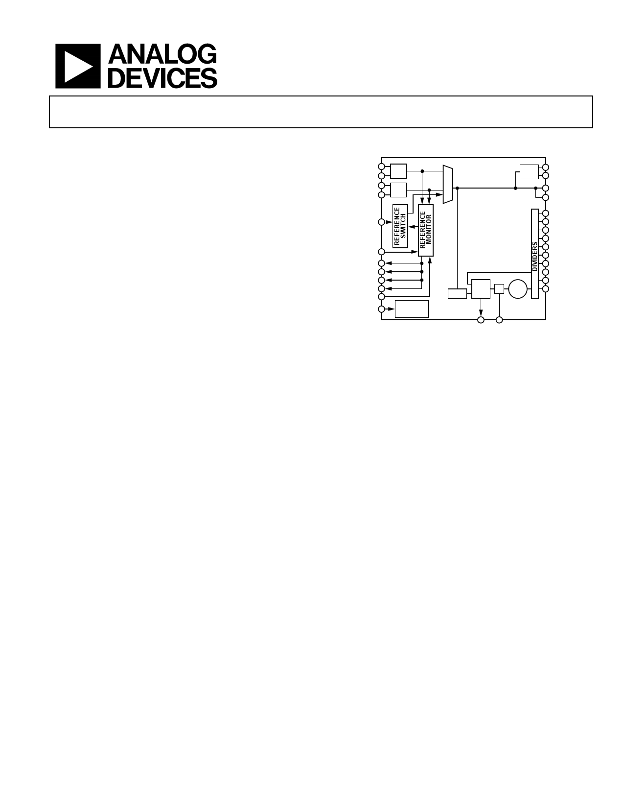
The AD9574 provides a multiple output clock generator function
comprising a dedicated phase-locked loop (PLL) core optimized
for Ethernet and gigabit Ethernet line card applications. The
integer-N PLL design is based on the Analog Devices, Inc.,
proven portfolio of high performance, low jitter frequency
synthesizers to maximize network performance. The AD9574
also benefits other applications requiring low phase noise and
jitter performance.
Configuring the AD9574 for a particular application requires
only the connection of external pull-up or pull-down resistors
to the appropriate pin program reader pins (PPRx). These pins
provide control of the internal dividers for establishing the
desired frequency translations, clock output functionality, and
input reference functionality. Connecting an external 19.44 MHz
or 25 MHz oscillator to one or both of the REF0_P/REF0_N or
REF1_P/REF1_N reference inputs results in a set of output
frequencies prescribed by the PPRx pins. Connecting a stable
FUNCTIONAL BLOCK DIAGRAM
REF0_P
REF0_N
REF1_P
REF1_N
Rx
Rx
REF_SEL
MCLK_x
REF_ACT
REF_SW
REF_FLO
REF_FHI
REFMON
PPRx
PPR
CONTROL
AD9574
×1/×2
×1/×2
PFD/
CP
LF
VCO
OUT0_P
OUT0_N
OUT1_P
OUT1_N
OUT2_P
OUT2_N
OUT3_P
OUT3_N
OUT4_P
OUT4_N
OUT5_P
OUT5_N
OUT6_P
OUT6_N
LD LF
Figure 1.
clock source (8 kHz/10 MHz/19.44 MHz/25 MHz/38.88 MHz) to
the monitor clock input enables the optional monitor circuit
providing quality of service (QoS) status for REF0 or REF1.
The PLL section consists of a low noise phase frequency
detector (PFD), a precision charge pump (CP), a partially
integrated loop filter (LF), a low phase noise voltage controlled
oscillator (VCO), and feedback and output dividers. The divider
values depend on the PPRx pins. The integrated loop filter
requires only a single external capacitor connected to the LF pin.
The AD9574 is packaged in a 48-lead 7 mm × 7 mm LFCSP,
requiring only a single 3.3 V supply. The operating temperature
range is −40°C to +85°C.
Note that throughout this data sheet, OUT0 to OUT6, REF0,
and REF1 refer to the respective channels, which consist of the
differential pins, OUT0_P/OUT0_N to OUT6_P/OUT6_N,
REF0_P/REF0_N, and REF1_P/REF1_N, respectively.
Rev. A
Document Feedback
Information furnished by Analog Devices is believed to be accurate and reliable. However, no
responsibility is assumed by Analog Devices for its use, nor for any infringements of patents or other
rights of third parties that may result from its use. Specifications subject to change without notice. No
license is granted by implication or otherwise under any patent or patent rights of Analog Devices.
Trademarksandregisteredtrademarksarethepropertyoftheirrespectiveowners.
One Technology Way, P.O. Box 9106, Norwood, MA 02062-9106, U.S.A.
Tel: 781.329.4700 ©2014–2015 Analog Devices, Inc. All rights reserved.
Technical Support
www.analog.com
1 page 
AD9574
Data Sheet
OUT4 AND OUT5 CHANNELS ABSOLUTE CLOCK JITTER
Typical values applicable under the conditions of VS = 3.3 V, TA = 25°C. Frequency multiplier (×2) at PLL input enabled unless otherwise
indicated.
Table 4.
Parameter
HSTL INTEGRATED JITTER
Jitter Integration Bandwidth = 10 kHz to 10 MHz
38.88 MHz Output
77.76 MHz Output
80 MHz Output
100 MHz Output
125 MHz Output
160 MHz Output
312.5 MHz Output
Jitter Integration Bandwidth = 12 kHz to 20 MHz
77.76 MHz Output
80 MHz Output
100 MHz Output
125 MHz Output
160 MHz Output
312.5 MHz Output
Jitter Integration Bandwidth = 50 kHz to 80 MHz
312.5 MHz Output
Jitter Integration Bandwidth = 1.875 MHz to 20 MHz
77.76 MHz Output
80 MHz Output
100 MHz Output
125 MHz Output
160 MHz Output
312.5 MHz Output
HIGH SPEED CURRENT SINKING LOGIC (HCSL) INTEGRATED
JITTER
Jitter Integration Bandwidth = 10 kHz to 10 MHz
100 MHz Output
125 MHz Output
312.5 MHz Output
Jitter Integration Bandwidth = 12 kHz to 20 MHz
100 MHz Output
125 MHz Output
312.5 MHz Output
Jitter Integration Bandwidth = 50 kHz to 80 MHz
312.5 MHz Output
Jitter Integration Bandwidth = 1.875 MHz to 20 MHz
100 MHz Output
125 MHz Output
312.5 MHz Output
Min
Typ Max
0.251
0.245
1.267
0.240
0.228
1.277
0.234
0.488
1.314
0.252
0.233
1.321
0.236
0.389
0.430
1.242
0.115
0.089
1.248
0.072
0.238
0.226
0.240
0.255
0.233
0.243
0.445
0.131
0.098
0.082
Unit Test Conditions/Comments
Input = crystal oscillator
ps rms
ps rms
ps rms
ps rms
ps rms
ps rms
ps rms
Frequency multiplier (×2) at PLL
input bypassed
Frequency multiplier (×2) at PLL
input bypassed
ps rms
ps rms
ps rms
ps rms
ps rms
ps rms
Frequency multiplier (×2) at PLL
input bypassed
Frequency multiplier (×2) at PLL
input bypassed
ps rms
ps rms
ps rms
ps rms
ps rms
ps rms
ps rms
Frequency multiplier (×2) at PLL
input bypassed
Frequency multiplier (×2) at PLL
input bypassed
Input = crystal oscillator
ps rms
ps rms
ps rms
ps rms
ps rms
ps rms
ps rms
ps rms
ps rms
ps rms
Rev. A | Page 4 of 35
5 Page 
AD9574
Data Sheet
STATUS PINS
Typical is given for VS = 3.3 V ± 10%, TA = 25°C, unless otherwise noted. Minimum and maximum values are given over full VS and TA
(−40°C to +85°C) variation.
Table 14.
Parameter
OUTPUT CHARACTERISTICS
LD Pin
Logic 1 Voltage
Logic 0 Voltage
REF_ACT Pin
Logic 1 Voltage
Logic 0 Voltage
REF_SW Pin
Logic 1 Voltage
Logic 0 Voltage
REF_FHI Pin
Logic 1 Voltage
Logic 0 Voltage
REF_FLO Pin
Logic 1 Voltage
Logic 0 Voltage
Min
2.0
2.0
2.0
2.0
2.0
Typ Max
0.8
0.8
0.8
0.8
0.8
Unit
Test Conditions/Comments
ILOAD = 1 mA (source or sink)
V
V
V
V
V
V
Internal 30 kΩ pull-down resistor
V
V
Internal 30 kΩ pull-down resistor
V
V
POWER SUPPLY AND DISSIPATION
Typical is given for VS = 3.3 V ± 10%, TA = 25°C, unless otherwise noted. Minimum and maximum values are given over full VS and TA
(−40°C to +85°C) variation.
Table 15.
Parameter
POWER SUPPLY VOLTAGE
POWER DISSIPATION
Typical Configuration
All Blocks Running
Min Typ Max Unit Test Conditions/Comments
2.97 3.3 3.63 V
466 569 654
579 698 803
mW PPR0 State 0 (REF0_x: 25 MHz, 3.3 V CMOS buffer; REF1_x: no connection)
PPR1 State 0 (PLL input ×2: off; OUT2: 156.25 MHz, HSTL; OUT3: 156.25 MHz, HSTL)
PPR2 State 7 (OUT0: 25 MHz, HSTL, ×2 off; OUT1: disabled)
PPR3 State 0 (OUT4: 100 MHz, HSTL; OUT5: 125 MHz, HSTL)
PPR4 State 5 (OUT6: 66.67 MHz, 3.3 V CMOS)
PPR5 State 0 (reference monitor threshold: not applicable (25 ppm))
PPR6 State 0 (MCLK_x: no connection (19.44 MHz differential))
REFMON: GND
mW PPR0 State 4 (REF0_x: 25 MHz, differential; REF1_x: 25 MHz, differential)
PPR1 State 0 (PLL input ×2: off; OUT2: 156.25 MHz, HSTL; OUT3: 156.25 MHz, HSTL)
PPR2 State 2 (OUT0: 50 MHz, 3.3 V CMOS, ×2 on; OUT1: 25 MHz, 3.3 V CMOS)
PPR3 State 2 (OUT4: 100 MHz, HCSL; OUT5: 125 MHz, HSTL)
PPR4 State 1 (OUT6: 133.33 MHz, 3.3 V CMOS)
PPR5 State 6 (reference monitor threshold: 100 ppm)
PPR6 State 4 (MCLK_x: 38.88 MHz, differential)
REFMON: VDD
Rev. A | Page 10 of 35
11 Page | ||
| Páginas | Total 30 Páginas | |
| PDF Descargar | [ Datasheet AD9574.PDF ] | |
Hoja de datos destacado
| Número de pieza | Descripción | Fabricantes |
| AD9571 | Ethernet Clock Generator | Analog Devices |
| AD9572 | Fiber Channel/Ethernet Clock Generator IC | Analog Devices |
| AD9573 | PCI-Express Clock Generator IC | Analog Devices |
| AD9574 | Ethernet/Gigabit Ethernet Clock Generator | Analog Devices |
| Número de pieza | Descripción | Fabricantes |
| SLA6805M | High Voltage 3 phase Motor Driver IC. |
Sanken |
| SDC1742 | 12- and 14-Bit Hybrid Synchro / Resolver-to-Digital Converters. |
Analog Devices |
|
DataSheet.es es una pagina web que funciona como un repositorio de manuales o hoja de datos de muchos de los productos más populares, |
| DataSheet.es | 2020 | Privacy Policy | Contacto | Buscar |