|
|
|
PDF ADSP-21160MKB-80 Data sheet ( Hoja de datos )
| Número de pieza | ADSP-21160MKB-80 | |
| Descripción | DSP Microcomputer | |
| Fabricantes | Analog Devices | |
| Logotipo | ||
Hay una vista previa y un enlace de descarga de ADSP-21160MKB-80 (archivo pdf) en la parte inferior de esta página. Total 30 Páginas | ||
|
No Preview Available !
a
Preliminary Technical Data
DSP
Microcomputer
ADSP-21160
SUMMARY
• High performance 32-bit DSP—applications in
audio, medical, military, graphics, imaging, and
communication
• Super Harvard Architecture—four independent
buses for dual data fetch, instruction fetch, and
nonintrusive, zero-overhead I/O
• Backwards compatible—assembly source level
compatible with code for ADSP-2106x DSPs
• Single-Instruction-Multiple-Data (SIMD) com-
putational architecture—two 32-bit IEEE float-
ing-point computation units, each with a
multiplier, ALU, shifter, and register file
• Integrated peripherals—integrated I/O proces-
sor, 4 Mbit on-chip dual-ported SRAM, glueless
multiprocessing features, and ports (serial, link,
external bus, & JTAG)
KEY FEATURES
• 80 MHz (12.5 ns) or 100 MHz (10 ns) core
instruction rate
• Single-cycle instruction execution, including
SIMD operations in both computational units
• 600 MFLOPS peak and 400 MFLOPS sustained
performance (based on FIR)
• Dual Data Address Generators (DAGs) with
modulo and bit-reverse addressing
• Zero-overhead looping and single-cycle loop set-
up, providing efficient program sequencing
• IEEE 1149.1 JTAG standard test access port and
on-chip emulation
• 400-ball 27×27mm PBGA package
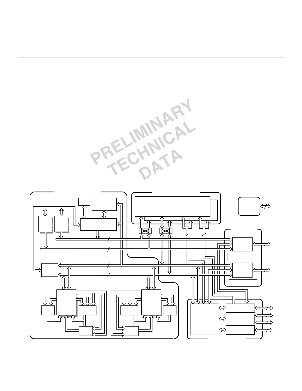
CORE PROCESSOR
TIMER INSTRUCTION
CACHE
32 x 48-BIT
DAG1
8x4x32
DAG2
8x4x32
PROGRAM
SEQUENCER
PM ADDRESS BUS
32
DM ADDRESS BUS
32
BUS
CONNECT
(PX)
PM DATA BUS 16/32/40/48/64
DM DATA BUS
32/40/64
DUAL-PORTED SRAM
TWO INDEPENDENT
DUAL-PORTED BLOCKS
PROCESSOR PORT
ADDR
DATA
ADDR
DATA
I/O PORT
DATA
ADDR
DATA
ADDR
IOD
64
IOA
18
JTAG
TEST &
EMULATION
6
EXTERNAL
PORT
ADDR BUS
MUX
32
MULTIPROCESSOR
INTERFACE
DATA BUS
MUX
64
HOST PORT
MULT
DATA
REGISTER
FILE
(PEx)
16 x 40-BIT
BARREL
SHIFTER
ALU
BARREL
SHIFTER
DATA
REGISTER
FILE
(PEy)
16 x 40-BIT
MULT
ALU
IOP
REGISTERS
(MEMORY MAPPED)
CONTROL,
STATUS, &
DATA BUFFERS
DMA
CONTROLLER
SERIAL PORTS
(2)
LINK PORTS
(6)
I/O PROCESSOR
Figure 1 ADSP-21160 Functional Block Diagram
4
6
6
60
REV. PrE
This information applies to a product under development. Its characteristics and
specifications are subject to change without notice. Analog Devices assumes no
obligation regarding future manufacturing unless otherwise agreed to in writing.
One Technology Way
P.O. Box 9106
Norwood MA 02062-9106
U.S.A.
http://www.analog.com/dsp
Tel: 1-800-ANALOG-D
Fax: 1-781-461-3010
Analog Devices Inc., 1998
1 page 
ADSP-21160 Preliminary Data Sheet
For current information contact Analog Devices at (781) 461-3881
January 2000
Entering SIMD mode also has an effect on the way data is transferred between memory and the
processing elements. When in SIMD mode, twice the data bandwidth is required to sustain
computational operation in the processing elements. Because of this requirement, entering SIMD mode
also doubles the bandwidth between memory and the processing elements. When using the DAGs to
transfer data in SIMD mode, two data values are transferred with each access of memory or the register
file.
Independent, Parallel Computation Units
Within each processing element is a set of computational units. The computational units consist of an
arithmetic/logic unit (ALU), multiplier and shifter. These units perform single-cycle instructions. The
three units within in each processing element are arranged in parallel, maximizing computational
throughput. Single multi-function instructions execute parallel ALU and multiplier operations. In
SIMD mode, the parallel ALU and multiplier operations occur in both processing elements. These
computation units support IEEE 32-bit single-precision floating-point, 40-bit extended precision
floating-point, and 32-bit fixed-point data formats.
Data Register File
A general purpose data register file is contained in each processing element. The register files transfer
data between the computation units and the data buses, and store intermediate results. These 10-port,
32-register (16 primary, 16 secondary) register files, combined with the ADSP-21100 enhanced
Harvard architecture, allows unconstrained data flow between computation units and internal memory.
The registers in PEX are referred to as R0-R15 and in PEY as S0-S15.
Single-Cycle Fetch of Instruction and Four Operands
The ADSP-21160 features an enhanced Harvard architecture in which the data memory (DM) bus
transfers data and the program memory (PM) bus transfers both instructions and data (see Figure 1).
With the ADSP-21160’s separate program and data memory buses and on-chip instruction cache, the
processor can simultaneously fetch four operands and an instruction (from the cache), all in a single
cycle.
Instruction Cache
The ADSP-21160 includes an on-chip instruction cache that enables three-bus operation for fetching
an instruction and four data values. The cache is selective—only the instructions whose fetches conflict
with PM bus data accesses are cached. This cache allows full-speed execution of core, looped operations
such as digital filter multiply-accumulates and FFT butterfly processing.
Data Address Generators With Hardware Circular Buffers
The ADSP-21160’s two data address generators (DAGs) are used for indirect addressing and let you
implement circular data buffers in hardware. Circular buffers allow efficient programming of delay lines
and other data structures required in digital signal processing, and are commonly used in digital filters
and Fourier transforms. The two DAGs of the ADSP-21160 contain sufficient registers to allow the
creation of up to 32 circular buffers (16 primary register sets, 16 secondary). The DAGs automatically
handle address pointer wrap-around, reducing overhead, increasing performance, and simplifying
implementation. Circular buffers can start and end at any memory location.
REV. PrE
This information applies to a product under development. Its characteristics and specifications are subject to change with-
out notice. Analog Devices assumes no obligation regarding future manufacturing unless otherwise agreed to in writing.
5
5 Page 
ADSP-21160 Preliminary Data Sheet
For current information contact Analog Devices at (781) 461-3881
January 2000
Note that the analog supply (AVDD) powers the ADSP-21160’s clock generator PLL. To produce a
stable clock, you must provide an external circuit to filter the power input to the AVDD pin. Place the
filter as close as possible to the pin. For an example circuit, see Figure 6. To prevent noise coupling, use
a wide trace for the analog ground (AGND) signal and install a decoupling capacitor as close as possible
to the pin.
VDDINT
10 Ω
0.1 µF
0.01 µF
AVDD
AGND
Figure 6 Analog Power (AVDD) Filter Circuit
Development Tools
The ADSP-21160 is supported with a complete set of VisualDSP® software and hardware development
tools, including the EZ-ICE® In-Circuit Emulator and development software. The same EZ-ICE
hardware that you use for the ADSP-21060/62, also fully emulates the ADSP-21160.
Both the SHARC Development Tools family and the VisualDSP integrated project management and
debugging environment support the ADSP-21160. The VisualDSP project management environment
enables you to develop and debug an application from within a single integrated program.
The SHARC Development Tools include an easy to use Assembler that is based on an algebraic syntax;
an Assembly library/librarian; a linker; a loader; a cycle-accurate, instruction-level simulator; a C
compiler; and a C run-time library that includes DSP and mathematical functions.
Debugging both C and Assembly programs with the Visual DSP debugger, you can:
• View mixed C and Assembly code
• Insert break points
• Set conditional breakpoints on registers, memory, and stacks
• Trace instruction execution
• Profile program execution
• Fill and dump memory
• Source level debugging
• Create custom debugger windows
The VisualDSP IDE lets you define and manage DSP software development. Its dialog boxes and
property pages enable you to configure and manage all of the SHARC Development Tools, including
the syntax highlighting in the VisualDSP editor. This capability lets you:
• Control how the development tools process inputs and generate outputs.
• Maintain a one-to-one correspondence with the tool’s command line switches.
The EZ-ICE Emulator uses the IEEE 1149.1 JTAG test access port of the ADSP-21160 processor to
monitor and control the target board processor during emulation. The EZ-ICE provides full-speed
REV. PrE
This information applies to a product under development. Its characteristics and specifications are subject to change with-
out notice. Analog Devices assumes no obligation regarding future manufacturing unless otherwise agreed to in writing.
11
11 Page | ||
| Páginas | Total 30 Páginas | |
| PDF Descargar | [ Datasheet ADSP-21160MKB-80.PDF ] | |
Hoja de datos destacado
| Número de pieza | Descripción | Fabricantes |
| ADSP-21160MKB-80 | Digital Signal Processor | Analog Devices |
| ADSP-21160MKB-80 | DSP Microcomputer | Analog Devices |
| Número de pieza | Descripción | Fabricantes |
| SLA6805M | High Voltage 3 phase Motor Driver IC. |
Sanken |
| SDC1742 | 12- and 14-Bit Hybrid Synchro / Resolver-to-Digital Converters. |
Analog Devices |
|
DataSheet.es es una pagina web que funciona como un repositorio de manuales o hoja de datos de muchos de los productos más populares, |
| DataSheet.es | 2020 | Privacy Policy | Contacto | Buscar |