|
|
|
PDF ADP3418 Data sheet ( Hoja de datos )
| Número de pieza | ADP3418 | |
| Descripción | 12V MOSFET Driver | |
| Fabricantes | ON Semiconductor | |
| Logotipo | ||
Hay una vista previa y un enlace de descarga de ADP3418 (archivo pdf) en la parte inferior de esta página. Total 13 Páginas | ||
|
No Preview Available !
Dual Bootstrapped, 12 V MOSFET
Driver with Output Disable
ADP3418
FEATURES
All-in-one synchronous buck driver
Bootstrapped high-side drive
1 PWM signal generates both drives
Anticross-conduction protection circuitry
Output disable control turns off both MOSFETs to float the
output per Intel® VR 10 and AMD Opteron™ specifications
APPLICATIONS
Multiphase desktop CPU supplies
Single-supply synchronous buck converters
GENERAL DESCRIPTION
The ADP3418 is a dual, high voltage MOSFET driver optimized
for driving two N-channel MOSFETs, the two switches in a
nonisolated, synchronous, buck power converter. Each of the
drivers is capable of driving a 3000 pF load with a 30 ns
transition time. One of the drivers can be bootstrapped and is
designed to handle the high voltage slew rate associated with
floating high-side gate drivers. The ADP3418 includes
overlapping drive protection to prevent shoot-through current
in the external MOSFETs. The OD pin shuts off both the high-
side and the low-side MOSFETs to prevent rapid output
capacitor discharge during system shutdowns.
The ADP3418 is specified over the commercial temperature
range of 0°C to 85°C and is available in an 8-lead SOIC package.
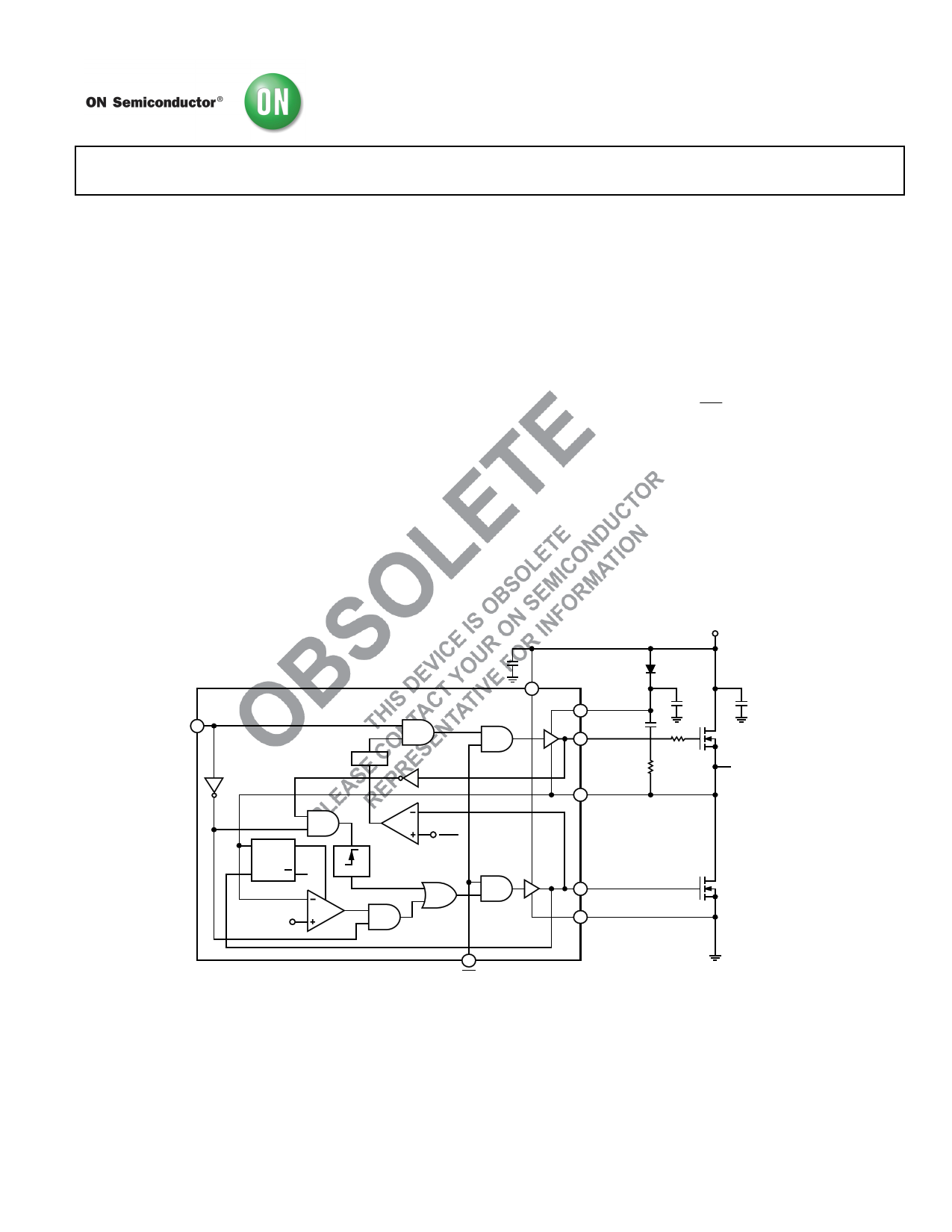
FUNCTIONAL BLOCK DIAGRAM
12V
ADP3418
IN 2
DELAY
SQ
RQ
CMP
DELAY
CMP
1V
CVCC
VCC
6
VCC
4
D1
BST
1
CBST1
DRVH
8
RBST1
SW
7
DRVL
5
PGND
6
CBST2
Q1
RG
TO
INDUCTOR
Q2
3
OD
Figure 1.
©2010 SCILLC. All rights reserved.
May 2010 – Rev. 6
Publication Order Number:
ADP3418/D
1 page 
PIN CONFIGURATION AND FUNCTION DESCRIPTIONS
ADP3418
BST 1
8 DRVH
IN 2 AD3418 7 SW
TOP VIEW
OD 3 (Not to Scale) 6 PGND
VCC 4
5 DRVL
Figure 2. Pin Configuration
Table 3. Pin Function Descriptions
Pin No. Mnemonic Description
1 BST
Upper MOSFET Floating Bootstrap Supply. A capacitor connected between the BST and SW pins holds this
bootstrapped voltage for the high-side MOSFET as it is switched. The capacitor should be between 100 nF and 1 µF.
2 IN
Logic Level Input. This pin has primary control of the drive outputs.
3 OD
Output Disable. When low, this pin disables normal operation, forcing DRVH and DRVL low.
4 VCC
Input Supply. This pin should be bypassed to PGND with a ~1 µF ceramic capacitor.
5 DRVL Synchronous Rectifier Drive. Output drive for the lower (synchronous rectifier) MOSFET.
6
PGND
Power Ground. Should be closely connected to the source of the lower MOSFET.
7 SW
This pin is connected to the buck switching node, close to the upper MOSFET’s source. It is the floating return
for the upper MOSFET drive signal.
8
DRVH
Buck Drive. Output drive for the upper (buck) MOSFET.
Rev. 6 | Page 5 of 13 | www.onsemi.com
5 Page 
ADP3418
The MOSFET vendor should provide a maximum voltage slew
rate at the drain current rating such that this can be designed
around. Once this specification is had, the next step is to
determine the maximum current expected to be seen in the
MOSFET. This can be done by
( )IMAX
= IDC ( per
phase) +
VCC − VOUT
×
D MAX
f MAX × LOUT
(5)
where:
DMAX is determined for the VR controller being used with the
driver. Note that this current is divided roughly equally between
MOSFETs if more than one is used (assume a worst-case mismatch
of 30% for design margin).
LOUT is the output inductor value.
When producing the design, there is no exact method for
calculating the dV/dt due to the parasitic effects in the external
MOSFETs as well as the PCB. However, it can be measured to
determine if it is safe. If it appears the dV/dt is too fast, an
optional gate resistor can be added between DRVH and the
high-side MOSFETs. This resistor slows down the dV/dt, but it
also increases the switching losses in the high-side MOSFETs.
The ADP3418 has been optimally designed with internal drive
impedance that works with most MOSFETs to switch them
efficiently while minimizing dV/dt. However, some high speed
MOSFETs can require this external gate resistor, depending on
the currents being switched in the MOSFET.
LOW-SIDE (SYNCHRONOUS) MOSFETS
The low-side MOSFETs are usually selected to have a low on
resistance to minimize conduction losses. This usually implies a
large input gate capacitance and gate charge. The first concern is
to make sure the power delivery from the ADP3418’s DRVL
does not exceed the thermal rating of the driver (see any ADI
Flex-Mode controller data sheet for details).
The next concern for the low-side MOSFETs is based on
preventing them from inadvertently being switched on when
the high-side MOSFET turns on. This occurs due to the drain-
gate (Miller, also specified as Crss) capacitance of the MOSFET.
When the drain of the low-side MOSFET is switched to VCC by
the high-side turning on (at a rate dV/dt), the internal gate of
the low-side MOSFET is pulled up by an amount roughly equal
to VCC × (Crss/Ciss). It is important to make sure this does not put
the MOSFET into conduction.
Another consideration is the nonoverlap circuitry of the
ADP3418, which attempts to minimize the nonoverlap period.
During the state of the high-side turning off to low-side turning
on, the SW pin is monitored (as well as the conditions of SW
prior to switching) to adequately prevent overlap.
However, during the low-side turn off to high-side turn on, the
SW pin does not contain information for determining the
proper switching time; therefore, the state of the DRVL pin is
monitored to go below one sixth of VCC and then a delay is
added. However, due to the Miller capacitance and internal
delays of the low-side MOSFET gate, one must ensure that the
Miller to input capacitance ratio is low enough, and that the
low-side MOSFET internal delays are not large enough, to allow
accidental turn on of the low-side when the high-side turns on.
A spreadsheet is available from ADI to assist designers with the
proper selection of low-side MOSFETs.
PC BOARD LAYOUT CONSIDERATIONS
Use the following general guidelines when designing printed
circuit boards:
• Trace out the high current paths and use short, wide
(>20 mil) traces to make these connections.
• Connect the PGND pin of the ADP3418 as close as
possible to the source of the lower MOSFET.
• The VCC bypass capacitor should be located as close as
possible to the VCC and PGND pins.
• Use vias to other layers when possible to maximize thermal
conduction away from the IC.
The circuit in Figure 15 shows how four drivers can be
combined with the ADP3188 to form a total power conversion
solution for generating VCC (CORE) for an Intel CPU that is VR
10.x-compliant.
Figure 14 shows an example of the typical land patterns based
on the guidelines given previously. For more detailed layout
guidelines for a complete CPU voltage regulator subsystem,
refer to the ADP3188 data sheet.
CBST1
CBST2
RBST
D1
CVCC
Figure 14. External Component Placement Example for the ADP3418 Driver
Rev. 6 | Page 11 of 13 | www.onsemi.com
11 Page | ||
| Páginas | Total 13 Páginas | |
| PDF Descargar | [ Datasheet ADP3418.PDF ] | |
Hoja de datos destacado
| Número de pieza | Descripción | Fabricantes |
| ADP3410 | Dual MOSFET Driver with Bootstrapping | Analog Devices |
| ADP3410KRU | Dual MOSFET Driver with Bootstrapping | Analog Devices |
| ADP3412 | Dual MOSFET Driver with Bootstrapping | Analog Devices |
| ADP3412JR | Dual MOSFET Driver with Bootstrapping | Analog Devices |
| Número de pieza | Descripción | Fabricantes |
| SLA6805M | High Voltage 3 phase Motor Driver IC. |
Sanken |
| SDC1742 | 12- and 14-Bit Hybrid Synchro / Resolver-to-Digital Converters. |
Analog Devices |
|
DataSheet.es es una pagina web que funciona como un repositorio de manuales o hoja de datos de muchos de los productos más populares, |
| DataSheet.es | 2020 | Privacy Policy | Contacto | Buscar |