|
|
|
PDF PC33981 Data sheet ( Hoja de datos )
| Número de pieza | PC33981 | |
| Descripción | Self-Protected High-Side Switch | |
| Fabricantes | Freescale Semiconductor | |
| Logotipo | ||
Hay una vista previa y un enlace de descarga de PC33981 (archivo pdf) en la parte inferior de esta página. Total 24 Páginas | ||
|
No Preview Available !
MOTOROLA
Freescale Semiconductor, Inc.
SEMICONDUCTOR TECHNICAL DATA
Document order number: MC33981
Rev 2.0, 10/2004
Preliminary Information
High-Frequency, High-Current,
Self-Protected High-Side Switch
(4.0 mΩ up to 60 kHz)
The 33981 is a high-frequency, self-protected 4.0 mΩ RDS(ON) high-side
switch used to replace electromechanical relays, fuses, and discrete devices
in power management applications.
The 33981 can be controlled by pulse-width modulation (PWM) with a
frequency up to 60 kHz. It is designed for harsh environments, and it includes
self-recovery features. The 33981 is suitable for loads with high inrush current,
as well as motors and all types of resistive and inductive loads.
The 33981 is packaged in a 12 x 12 nonleaded power-enhanced Power
QFN package with exposed tabs.
Features
• Single 4.0 mΩ RDS(ON) Maximum High-Side Switch
• PWM Capability up to 60 kHz with Duty Cycle from 5% to 100%
• Very Low Standby Current
• Slew Rate Control with External Capacitor
• Overcurrent and Overtemperature Protection, Undervoltage Shutdown
and Fault Reporting
• Reverse Battery Protection
• Gate Drive Signal for External Low-Side N-Channel MOSFET with
Protection Features
• Output Current Monitoring
• Temperature Feedback
33981
HIGH-SIDE SWITCH
4.0 mΩ
Bottom View
PNA SUFFIX
SCCAASEL1E4021-0:21
16-TERMINAL PQFN (12 X 12)
ORDERING INFORMATION
Device
Temperature
Range (TA)
Package
PC33981PNA/R2 -40°C to 125°C 16 PQFN
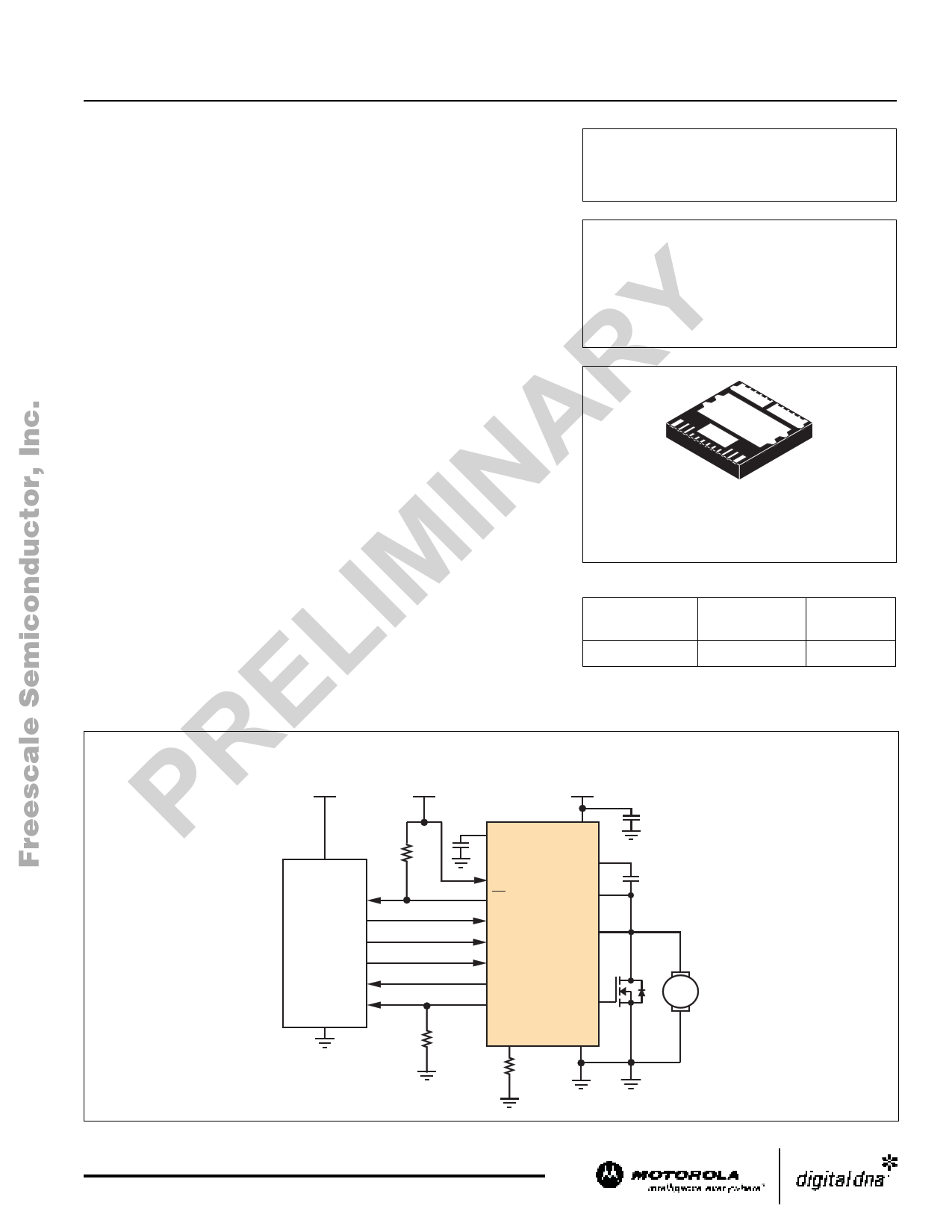
33981 SimplifieSdimAplpifpieldicAaptpiolincaDtioiangDriaamgram
VDD VDD
I/O
I/O
MCU I/O
I/O
A/D
A/D
VPWR
33981
SR
CONF
FS
INLS
EN
INHS
TEMP
CSNS
VPWR
CBOOT
OUT
DLS
GLS
OCLS GND
M
This document contains information on a product under development.
Motorola reserves the right to change or discontinue this product without notice.
© Motorola, Inc. 2004
For More Information On This Product,
Go to: www.freescale.com
http://www.Datasheet4U.com/
1 page 
Freescale Semiconductor, Inc.
MAXIMUM RATINGS
All voltages are with respect to ground unless otherwise noted.
Rating
Symbol
Value
Unit
ELECTRICAL RATINGS
Power Supply Voltage
Steady-State
VPWR
-16 to 41
V
Input/Output Terminals Voltage (Note 1)
Output Voltage
Continuous Output Current (Note 2) I
CSNS Input Clamp Current
SR Voltage
Temperature Feedback Voltage
CBOOT Voltage
VIN
VOUT
OUT
ICSNS
VSR
VTEMP
CBOOT
-0.3 to 7.0
-5.0 to 41
40
10
-0.3 to 54
-0.3 to 5.0
-0.3 to 54
V
V
A
mA
V
V
V
OCLS Voltage
Low-Side Gate Voltage
Low-Side Drain Voltage
ESD Voltage
Human Body Model (Note 3)
Machine Model (Note 4)
VOCLS
VGLS
VDLS
VESD1
VESD2
-0.3 to 7.0
-0.3 to 15
-5.0 to 41
± 2000
± 200
V
V
V
V
Output Clamp Energy (Note 5)
ECL
TBD
J
THERMAL RATINGS
Operating Temperature
Ambient
Junction
Storage Temperature
Thermal Resistance (Note 6)
Junction to Power Die Case
Junction to Ambient
Peak Terminal Reflow Temperature During Solder Mounting (Note 7)
Power Dissipation (TA = 25°C) (Note 8)
TA
TJ
TSTG
RθJC
RθJA
TSOLDER
PD
-40 to 125
-40 to 150
-55 to 150
1.0
20
240
TBD
°C
°C
°C/W
°C
W
Notes
1. Exceeding voltage limits on INHS, INLS, CONF, CSNS, FS, TEMP, and EN terminals may cause a malfunction or permanent damage to the
device.
2. Continuous high-side output rating as long as maximum junction temperature is not exceeded. Calculation of maximum output current using
package thermal resistance is required.
3. ESD1 testing is performed in accordance with the Human Body Model (CZAP = 100 pF, RZAP = 1500 Ω).
4. ESD2 testing is performed in accordance with the Machine Model (CZAP = 200 pF, RZAP = 0 Ω) and in accordance with the system module
specification with a capacitor > 0.01 µF connected from OUT to GND.
5. Active clamp energy using single-pulse method (L = 16 mH, RL = 0, VPWR = 12 V, TJ = 150°C).
6. Device mounted on a 2s2p test board per JEDEC JESD51-2.
7. Terminal soldering temperature limit is for 10 seconds maximum duration. Not designed for immersion soldering. Exceeding these limits may
cause malfunction or permanent damage to the device.
8. Maximum power dissipation at indicated ambient temperature in free air with no heatsink used.
MOTOROLA ANALOG INTEGRATED CIRCUIT DEVICE DATA
For More Information On This Product,
Go to: www.freescale.com
33981
5http://www.Datasheet4U.com/
5 Page 
Freescale Semiconductor, Inc.
Functional Diagrams
EN
CONF
INHS
High Side ON
High Side OFF
0V
INLS
OUT
Low Side ON
Thermal Shutdown on OUT
0V
GLS
FS
TEMP
Temperature
OUT
Thermal Shutdown on OUT
5.0 V
Thermal Shutdown on OUT
5.0 V
0V
Thermal Shutdown
on OUT
0V
Thermal Shutdown
on OUT
0V
Thermal Shutdown on OUT
TSD
High Side ON
Thermal Shutdown on OUT
High Side OFF
Hysteresis
TSD Hysteresis
Figure 3. Overtemperature on Output
MOTOROLA ANALOG INTEGRATED CIRCUIT DEVICE DATA
For More Information On This Product,
Go to: www.freescale.com
33981
11http://www.Datasheet4U.com/
11 Page | ||
| Páginas | Total 24 Páginas | |
| PDF Descargar | [ Datasheet PC33981.PDF ] | |
Hoja de datos destacado
| Número de pieza | Descripción | Fabricantes |
| PC33981 | Self-Protected High-Side Switch | Freescale Semiconductor |
| Número de pieza | Descripción | Fabricantes |
| SLA6805M | High Voltage 3 phase Motor Driver IC. |
Sanken |
| SDC1742 | 12- and 14-Bit Hybrid Synchro / Resolver-to-Digital Converters. |
Analog Devices |
|
DataSheet.es es una pagina web que funciona como un repositorio de manuales o hoja de datos de muchos de los productos más populares, |
| DataSheet.es | 2020 | Privacy Policy | Contacto | Buscar |