|
|
PDF PBL3799-2 Data sheet ( Hoja de datos )
| Número de pieza | PBL3799-2 | |
| Descripción | Subscriber Line Interface Circuit | |
| Fabricantes | Ericsson | |
| Logotipo |  |
|
Hay una vista previa y un enlace de descarga de PBL3799-2 (archivo pdf) en la parte inferior de esta página. Total 22 Páginas | ||
|
No Preview Available !
PABpLril31799997
www.DataSheet4U.com
PBL 3799, PBL 3799/2
Subscriber Line
Interface Circuit
Description
Key Features
PBL 3799 is an analog Subscriber Line Interface Circuit (SLIC), which is fabricated in a
75 V bipolar, monolithic process.
The programmable, resistive feed circuit incorporates a switch mode regulator to
minimize on-chip power dissipation. A stand-by state further reduces idle power
dissipation, while allowing the supervisory functions to be active.
Tip-ring polarity is reversible without altering SLIC supervisory and voice frequency
(vf) functions. Tip and ring outputs can be set to high impedance states. These and
other operating states are activated via a parallel, four bit control word.
An external resistor controls the off-hook detector threshold current. A ground key
detector with internal reference reports tip/ring dc current unbalance. The ring trip
detector can operate with both balanced and unbalanced ringing systems. The three
detectors are read via a shared output.
Ring and test relay drivers with internal clamp diodes are provided.
The complex or real two-wire impedance is set by a scaled, lumped element
network.
Two- to four-wire and four- to two-wire signal conversion is provided by the SLIC in
conjunction with either a conventional or a programmable CODEC/filter.
Longitudinal line voltages are suppressed by a control loop within the SLIC.
The PBL 3799 package is 28-pin, dual-in-line; 32-pin or 44-pin, j-leaded chip carrier.
The difference between PBL 3799 and PBL 3799/2 is mainly the longitudinal
balance spec.
6/4
RINGRLY
7/5
TESTRLY
40/26
DR
38/25
DT
42/27
TIPX
34/22
HPT
35/23
HPR
43/28
RINGX
3/2
VREG
L
VBAT
GND2
8/6
10/7
2/1
Ring Relay
Driver
Test Relay
Driver
Ring Trip
Comparator
Two-wire
Interface
Input
Decoder
and
Control
Loop/Gnd Key
Detector
VF Signal
Transmission
Line Feed
Controller and
Longitudinal
Suppression
Switching
Regulator
12/9 11/8 14/10
CHS VQBAT CHCLK
4/3
VCC
31/20
VEE
23/16
C1
21/14
C2
22/15
C3
16/11
C4
19/—
E0
17/12
E1
20/13
DET
37/24
RD
32/21
VTX
29/19
RSN
26/17
RDC
25/—
RSG
27/18
GND1
• On-chip switch mode regulator to
minimize power dissipation
• Programmable, resistive battery feed
• Line feed characteristics independ-
ent of battery variations
• Tip-ring polarity reversal function
• Tip and ring open circuit state; tip
open with ring active state
• Detectors:
- programmable loop current/ring
ground detector
- ground key detector
- ring trip detector
• Ring and test relay drivers
• Line terminating impedance,
complex or real, set by a simple
external network
• Hybrid function with conventional or
programmable CODEC/filters
• 70 dB longitudinal to metallic
balance
• 79 mA peak longitudinal current
suppression
• Idle noise < 10 dBrnC; < -80 dBup
PBL 3799
Figure 1. Block diagram.
4-191 http://www.Datasheet4U.com/
1 page 
PBL 3799
Parawmwetwer.DataSheet4U.com
2-wire return loss, r
Polarity reversal time, t
pol
TIPX idle voltage, VTi
TIPX to RINGX idle
voltage, Vtro
Standard version
-/2 version
4-wire Transmit Port (VTX)
Overload level, VTXO
Output offset voltage, ∆VTX
Output impedance, zTX
4-wire Receive Port (RSN)
RSN dc voltage, VRSN
RSN impedance, zRSN
RSN current (I ) to metallic
RSN
loop current (IL) gain, αRSN
Frequency Response
Two-wire to four-wire, g2-4
Four-wire to two-wire, g
4-2
Four-wire to four-wire, g4-4
Insertion Loss
Two-wire to four-wire, G2-4
Ref
fig Conditions
Min Typ Max
Z +Z
r = 20 • log L TR , Note 5
ZL - ZTR
0.2kHz ≤ f < 0.5kHz
30
37
0.5kHz ≤ f < 1.0kHz
25 33
1.0kHz ≤ f ≤ 3.4kHz
15 24
Normal to reversed polarity or
4 15
reversed to normal polarity
Normal polarity, Note 6
VBat = -48 V
V = -63 V
Bat
Active and standby
-5.0 -3.5 -2.0
-5.0 -3.5 -2.0
VBat = -48V,
R1 = open loop
Normal polarity
42
Reversed polarity
-42
Normal polarity
40
Reversed polarity
-40
2 Load impedance > 20 kohms,
f = 1 kHz, 1% THD, ERX = 0
Note 7
0.2kHz ≤ f ≤ 3.4kHz
3.1 3.5
9.0 10.1
-50 ±5 +50
10 20
IRSN = 0
0.2kHz ≤ f ≤ 3.4kHz
0.2kHz ≤ f ≤ 3.4kHz,
αRSN =
IL
IRSN
6 0.3kHz ≤ f ≤ 3.4kHz
Relative to 1.0 kHz, 0 dBu
ERX = 0 V, (Notes 2, 8)
6 0.3kHz ≤ f ≤ 3.4kHz
Relative to 1.0 kHz, 0 dBu
EL = 0 V, (Notes 2, 9)
6 0.3kHz ≤ f ≤ 3.4kHz
Relative to 1.0 kHz, 0 dBu
EL = 0 V, (Notes 2, 9)
6 0 dBu, 1 kHz, ERX = 0
(Notes 8, 10)
-10 0 +10
3 20
40
-0.1 ±0.03 +0.1
-0.1 ±0.03 +0.1
-0.1 ±0.06 +0.1
-0.15 ±0.1 +0.15
Unit
dB
dB
dB
ms
V
V
V
V
V
V
VPk
dBu
mV
ohm
mV
ohm
dB
dB
dB
dB
dB
C
+
RL
TIPX
42/27
VTX
32/21
TX
+
VTR
EL –
ILdc PBL 3799
RINGX
43/28
RSN
29/19
RT
RRX
RX
E RX
VTX
–
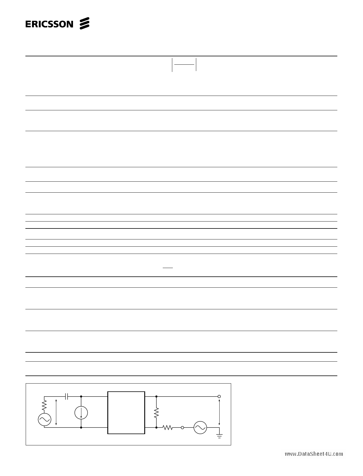
Figure 6. Frequency response, insertion
loss, gain tracking, idle channel noise,
THD, inter-modulation.
1/ωC << RL, RL = 600 ohms,
RT = 60 kohms, RRX = 30 kohms.
4-195 http://www.Datasheet4U.com/
5 Page 
PBL 3799
44 PwLCwCw.D3a2tPaLSChCeetP4DUI.Pcom Symbol
25 — — RSG
26 19 17 RDC
27 20&21 18 GND1
28 — — NC
29 22 19 RSN
30 — — NC
31 23 20 VEE
32 24 21 VTX
33 — — NC
34 25 22 HPT
35 26 23 HPR
Description
Saturation guard programming input. A resistor, RSG, between pins RSG and VEE adjusts
the saturation guard for operation with VBat from -64.5 V to -46 V, see battery feed page
15. The PBL 3799 in dual-in-line and 32-pin surface mount package has the saturation
guard internally set for operation with VBat = -48 V.
Dc loop feed resistance is programmed by two resistors connected in series from this pin
to the receive summing node (RSN). The resistor junction point is decoupled to GND1 to
filter noise and other disturbances before reaching the RSN input. VRDC polarity is
negative for normal tip-ring polarity and positive for reversed tip-ring polarity.
|VRDC| = |(|VTdc - V Rdc|/20) - 2.5|.
Ground. No internal connection to GND2. Note 2.
No internal connection. Note 1.
Receive summing node. 100 times the current (dc and ac) flowing into this pin equals the
metallic (transversal) current flowing between the TIPX and RINGX terminals. Program
ming networks for feed resistance, 2-wire impedance, and receive gain connect to the
receive summing node.
No internal connection. Note 1.
-5 V power supply.
Transmit vf output. The ac voltage difference between TIPX and RINGX, the ac metallic
voltage, is reproduced as an unbalanced GND1 referenced signal at VTX with a gain of
one. The two-wire impedance programming network connects between VTX and RSN.
No internal connection. Note 1.
Tip side (HPT) of ac/dc separation capacitor.
Ring side (HPR) of ac/dc separation capacitor.
TP 5
TESTRLY 6
L7
VBAT 8
VQBAT 9
CHS 10
CHCLK 11
C4 12
E1 13
29 TP
28 DT
27 RD
26 HPR
25 HPT
24 VTX
23 VEE
22 RSN
21 GND1
GND2 1
VREG 2
VCC 3
RINGRLY 4
TESTRLY 5
L6
VBAT 7
VQBAT 8
CHS 9
CHCLK 10
C4 11
E1 12
DET 13
C2 14
TESTRLY 7
L8
NC 9
VBAT 10
28 RINGX
VQBAT 11
CHS 12
27 TIPX
26 DR
25 DT
24 RD
23 HPR
NC 13
CHCLK 14
NC 15
C4 16
E1 17
22 HPT
21 VTX
20 VEE
19 RSN
18 GND1
17 RDC
16 C1
15 C3
39 NC
38 DT
37 RD
36 NC
35 HPR
34 HPT
33 NC
32 VTX
31 VEE
30 NC
29 RSN
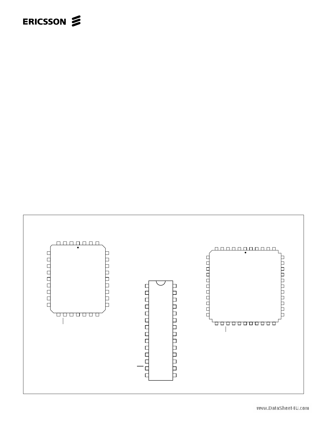
Figure 11. Pin configuration, 28-pin dual-in-line package, 32-pin j-leaded chip carrier and 44-pin j-leaded chip carrier, top view.
4-201 http://www.Datasheet4U.com/
11 Page | ||
| Páginas | Total 22 Páginas | |
| PDF Descargar | [ Datasheet PBL3799-2.PDF ] | |
Hoja de datos destacado
| Número de pieza | Descripción | Fabricantes |
| PBL3799-2 | Subscriber Line Interface Circuit | Ericsson |
| Número de pieza | Descripción | Fabricantes |
| SLA6805M | High Voltage 3 phase Motor Driver IC. |
Sanken |
| SDC1742 | 12- and 14-Bit Hybrid Synchro / Resolver-to-Digital Converters. |
Analog Devices |
|
DataSheet.es es una pagina web que funciona como un repositorio de manuales o hoja de datos de muchos de los productos más populares, |
| DataSheet.es | 2020 | Privacy Policy | Contacto | Buscar |
