|
|
|
PDF ADP2384 Data sheet ( Hoja de datos )
| Número de pieza | ADP2384 | |
| Descripción | Step-Down DC-to-DC Regulator | |
| Fabricantes | Analog Devices | |
| Logotipo | ||
Hay una vista previa y un enlace de descarga de ADP2384 (archivo pdf) en la parte inferior de esta página. Total 24 Páginas | ||
|
No Preview Available !
Data Sheet
20 V, 4 A, Synchronous, Step-Down
DC-to-DC Regulator
ADP2384
FEATURES
Input voltage: 4.5 V to 20 V
Integrated MOSFET: 44 mΩ/11.6 mΩ
Reference voltage: 0.6 V ± 1%
Continuous output current: 4 A
Programmable switching frequency: 200 kHz to 1.4 MHz
Synchronizes to external clock: 200 kHz to 1.4 MHz
180° out-of-phase clock synchronization
Precision enable and power good
External compensation
Internal soft start with external adjustable option
Startup into a precharged output
Supported by ADIsimPower design tool
APPLICATIONS
Communications infrastructure
Networking and servers
Industrial and instrumentation
Healthcare and medical
Intermediate power rail conversion
DC-to-dc point-of-load applications
GENERAL DESCRIPTION
The ADP2384 is a synchronous, step-down dc-to-dc regulator
with an integrated 44 mΩ, high-side power MOSFET and
an 11.6 mΩ, synchronous rectifier MOSFET to provide a high
efficiency solution in a compact 4 mm × 4 mm LFCSP package.
This device uses a peak current mode, constant frequency pulse-
width modulation (PWM) control scheme for excellent stability
and transient response. The switching frequency of the ADP2384
can be programmed from 200 kHz to 1.4 MHz. To minimize
system noise, the synchronization function allows the switching
frequency to be synchronized to an external clock.
The ADP2384 requires minimal external components and operates
from an input voltage of 4.5 V to 20 V. The output voltage can be
adjusted from 0.6 V to 90% of the input voltage and delivers up to
TYPICAL APPLICATIONS CIRCUIT
VIN
CIN
RT
CVREG
ADP2384
PVIN
BST
EN
PGOOD
SW
SYNC
RT
FB
COMP
VREG
SS
GND PGND
CBST L
RTOP
RC
CSS
RBOT
CC
VOUT
COUT
Figure 1.
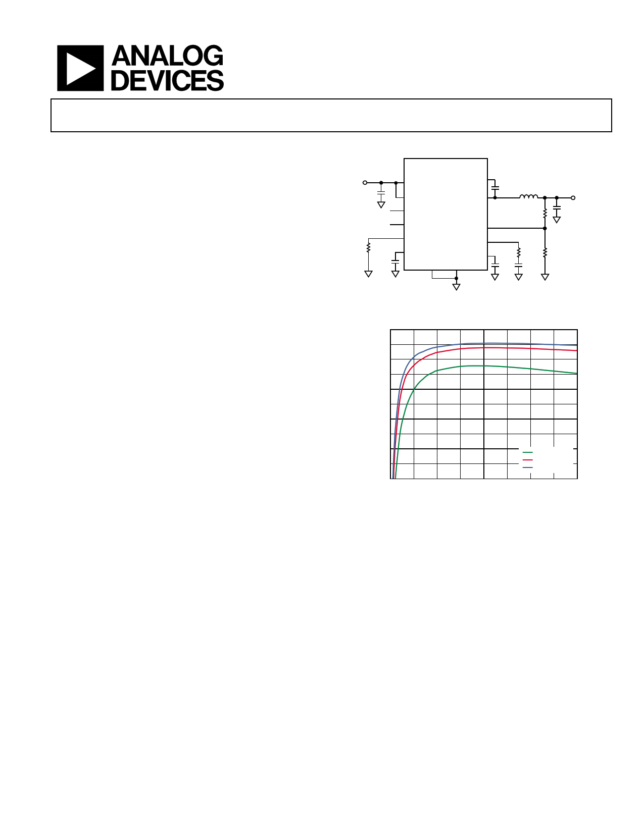
100
95
90
85
80
75
70
65
60 VOUT = 1.2V
55
VOUT = 3.3V
VOUT = 5V
50
0 0.5 1.0 1.5 2.0 2.5 3.0 3.5 4.0
OUTPUT CURRENT (A)
Figure 2. Efficiency vs. Output Current, VIN = 12 V, fSW = 300 kHz
4 A of continuous current. Each IC draws less than 120 μA current
from the input source when it is disabled.
This regulator targets high performance applications that require
high efficiency and design flexibility. External compensation and an
adjustable soft start function provide design flexibility. The power-
good output and precision enable input provide simple and reliable
power sequencing.
Other key features include undervoltage lockout (UVLO),
overvoltage protection (OVP), overcurrent protection (OCP),
short-circuit protection (SCP), and thermal shutdown (TSD).
The ADP2384 operates over the −40°C to +125°C junction
temperature range and is available in a 24-lead, 4 mm × 4 mm
LFCSP package.
Rev. 0
Information furnished by Analog Devices is believed to be accurate and reliable. However, no
responsibility is assumed by Analog Devices for its use, nor for any infringements of patents or other
rights of third parties that may result from its use. Specifications subject to change without notice. No
license is granted by implication or otherwise under any patent or patent rights of Analog Devices.
Trademarksandregisteredtrademarksarethepropertyoftheirrespectiveowners.
One Technology Way, P.O. Box 9106, Norwood, MA 02062-9106, U.S.A.
Tel: 781.329.4700
www.analog.com
Fax: 781.461.3113
©2012 Analog Devices, Inc. All rights reserved.
Free Datasheet http://www.Datasheet4U.com
1 page 
Data Sheet
ABSOLUTE MAXIMUM RATINGS
Table 2.
Parameter
PVIN, EN, PGOOD
SW
BST
FB, SS, COMP, SYNC, RT
VREG
PGND to GND
Operating Junction Temperature Range
Storage Temperature Range
Soldering Conditions
Rating
−0.3 V to +22 V
−1 V to +22 V
VSW + 6 V
−0.3 V to +6 V
−0.3 V to +12 V
−0.3 V to +0.3 V
−40°C to +125°C
−65°C to +150°C
JEDEC J-STD-020
Stresses above those listed under Absolute Maximum Ratings
may cause permanent damage to the device. This is a stress
rating only; functional operation of the device at these or any
other conditions above those indicated in the operational
section of this specification is not implied. Exposure to absolute
maximum rating conditions for extended periods may affect
device reliability.
ADP2384
THERMAL RESISTANCE
θJA is specified for the worst-case conditions, that is, a device
soldered in a 4-layer, JEDEC standard circuit board for surface-
mount packages.
Table 3. Thermal Resistance
Package Type
24-Lead LFCSP_WQ
θJA Unit
42.6 °C/W
ESD CAUTION
Rev. 0 | Page 5 of 24
Free Datasheet http://www.Datasheet4U.com
5 Page 
Data Sheet
FUNCTIONAL BLOCK DIAGRAM
VREG
RT
SYNC
EN
1.17V
OSC
CLK
SLOPE RAMP
EN_BUF
BIAS AND DRIVER
REGULATOR
UVLO
BOOST
REGULATOR
PVIN
1µA 4µA
COMP
SS
FB
SLOPE RAMP
0.6V
+
ISS
+ AMP
–
PGOOD
GND
0.7V –
+
–
0.54V
+
DEGLITCH
+
OCP
VI_MAX –
Σ
HICCUP
MODE
ACS
+
CMP
–
OVP
CLK
DRIVER
CONTROL
LOGIC
AND MOSFET
DRIVER WITH
ANTICROSS
PROTECTION
VREG
DRIVER
NEG CURRENT
CMP
–
+
BST
NFET
SW
NFET
PGND
VI_NEG
Figure 28. Functional Block Diagram
ADP2384
Rev. 0 | Page 11 of 24
Free Datasheet http://www.Datasheet4U.com
11 Page | ||
| Páginas | Total 24 Páginas | |
| PDF Descargar | [ Datasheet ADP2384.PDF ] | |
Hoja de datos destacado
| Número de pieza | Descripción | Fabricantes |
| ADP2380 | 4 A Synchronous Step-Down Regulator | Analog Devices |
| ADP2381 | 6 A Synchronous Step-Down Regulator | Analog Devices |
| ADP2384 | Step-Down DC-to-DC Regulator | Analog Devices |
| ADP2386 | Synchronous Step-Down DC-to-DC Regulator | Analog Devices |
| Número de pieza | Descripción | Fabricantes |
| SLA6805M | High Voltage 3 phase Motor Driver IC. |
Sanken |
| SDC1742 | 12- and 14-Bit Hybrid Synchro / Resolver-to-Digital Converters. |
Analog Devices |
|
DataSheet.es es una pagina web que funciona como un repositorio de manuales o hoja de datos de muchos de los productos más populares, |
| DataSheet.es | 2020 | Privacy Policy | Contacto | Buscar |