|
|
|
PDF ACT4065A Data sheet ( Hoja de datos )
| Número de pieza | ACT4065A | |
| Descripción | High Input 2A Step Down Converter | |
| Fabricantes | Active-Semi | |
| Logotipo | ||
Hay una vista previa y un enlace de descarga de ACT4065A (archivo pdf) en la parte inferior de esta página. Total 9 Páginas | ||
|
No Preview Available !
®
FEATURES
• 2A Output Current
• Up to 95% Efficiency
• 6.0V to 30V Input Range
• 210kHz Switching Frequency
• Adjustable Output Voltage
• Cycle-by-Cycle Current Limit Protection
• Thermal Shutdown Protection
• Frequency Foldback at Short Circuit
• Stability with Wide Range of Capacitors,
Including Low ESR Ceramic Capacitors
• SOP-8 Package
APPLICATIONS
• TFT LCD Monitors
• Portable DVDs
• Car-Powered or Battery-Powered Equip-
ments
• Set-Top Boxes
• Telecom Power Supplies
• DSL and Cable Modems and Routers
• Termination Supplies
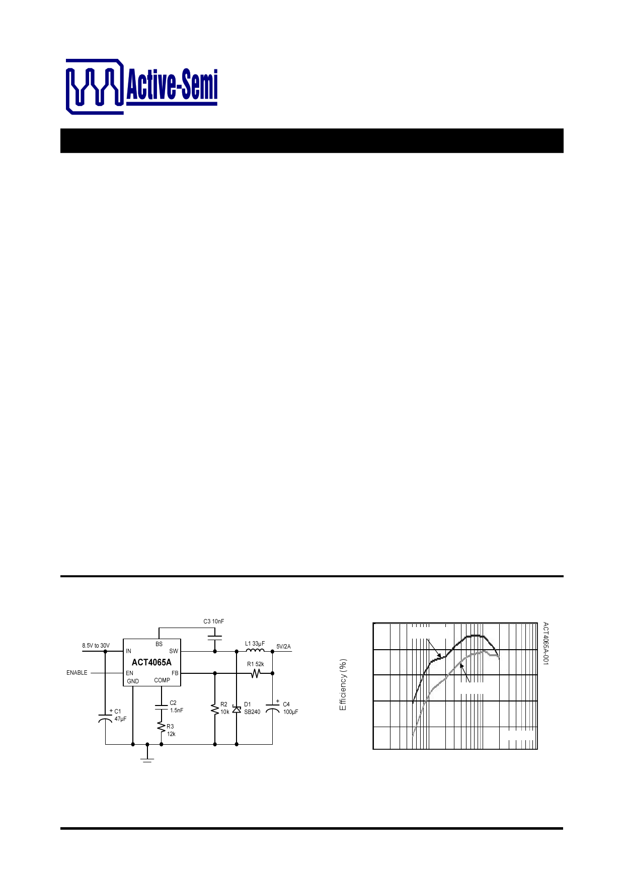
ACT4065A
Rev 0, 23-Apr-12
High Input 2A Step Down Converter
GENERAL DESCRIPTION
The ACT4065A is a current-mode step-down
DC/DC converter that generates up to 2A output
current at 210kHz switching frequency.
The ACT4065A is highly efficient with peak effi-
ciency at 95% when in operation. Protection fea-
tures include cycle-by-cycle current limit, thermal
shutdown, and frequency foldback at short circuit.
The ACT4065A is available in SOP-8 package and
requires very few external devices for operation.
Note: ACT4065A is the drop-in replacement for
ACT4065 with feedback resistance value change.
Innovative PowerTM
Efficiency vs. Load current
95
VIN = 12V
90
85
VIN = 24V
80
75
70
10
VOUT = 5V
100 1000
Load Current (mA)
10000
-1-
www.active-semi.com
Copyright © 2012 Active-Semi, Inc.
Free Datasheet http://www.Datasheet-PDF.com/
1 page 
® ACT4065A
Rev 0, 23-Apr-12
APPLICATIONS INFORMATION
Output Voltage Setting
Figure 1:
Output Voltage Setting
Figure 1 shows the connections for setting the out-
put voltage. Select the proper ratio of the two feed-
back resistors RFB1 and RFB2 based on the output
voltage. Typically, use RFB2 ≈ 10kΩ and determine
RFB1 from the output voltage:
RFB1
=
RFB2
⎜⎛
⎝
VOUT
0.808V
−1⎟⎞
⎠
(1)
Inductor Selection
The inductor maintains a continuous current to the
output load. This inductor current has a ripple that is
dependent on the inductance value: higher induc-
tance reduces the peak-to-peak ripple current. The
trade off for high inductance value is the increase in
inductor core size and series resistance, and the
reduction in current handling capability. In general,
select an inductance value L based on ripple current
requirement:
( )L
=
VOUT × VIN − VOUT
V f I KIN SW OUTMAX RIPPLE
(2)
where VIN is the input voltage, VOUT is the output
voltage, fSW is the switching frequency, IOUTMAX is the
maximum output current, and KRIPPLE is the ripple
factor. Typically, choose KRIPPLE = 30% to
correspond to the peak-to-peak ripple current being
30% of the maximum output current.
With this inductor value (Table 1), the peak inductor
current is IOUT × (1 + KRIPPLE / 2). Make sure that this
peak inductor current is less that the 3A current limit.
Finally, select the inductor core size so that it does
not saturate at 3A.
Input Capacitor
The input capacitor needs to be carefully selected to
maintain sufficiently low ripple at the supply input of
the converter. A low ESR capacitor is highly recom-
mended. Since a large current flows in and out of
this capacitor during switching, its ESR also affects
efficiency.
The input capacitance needs to be higher than
10µF. The best choice is the ceramic type; however,
low ESR tantalum or electrolytic types may also be
used provided that the RMS ripple current rating is
higher than 50% of the output current. The input
capacitor should be placed close to the IN and G
pins of the IC, with shortest possible traces. In the
case of tantalum or electrolytic types, they can be
further away if a small parallel 0.1µF ceramic ca-
pacitor is placed right next to the IC.
Output Capacitor
The output capacitor also needs to have low ESR to
keep low output voltage ripple. The output ripple
voltage is:
VRIPPLE
=
I K ROUTMAX RIPPLE ESR
+
⎜⎜⎝⎛
28
×
VIN
fSW 2LCOUT
⎟⎟⎠⎞
(3)
where IOUTMAX is the maximum output current,
KRIPPLE is the ripple factor, RESR is the ESR
resistance of the output capacitor, fSW is the
switching frequency, L is the inductor value, COUT is
the output capacitance, RESR is very small and does
not contribute to the ripple. Therefore, a lower ca-
pacitance value can be used for ceramic type. In the
case of tantalum or electrolytic type, the ripple is
dominated by RESR multiplied by the ripple current.
In that case, the output capacitor is chosen to have
sufficiently low ESR.
For ceramic output type, typically choose a
capacitance of about 22µF. For tantalum or
electrolytic type, choose a capacitor with less than
50mΩ ESR.
Rectifier Diode
Use a Schotky diode as the rectifier to conduct cur-
rent when the High-Side Power Switch is off. The
Schottky diode must have current rating higher than
the maximum output current and the reverse volt-
age rating higher than the maximum input voltage.
Table 1.
Typical Inductor Values
VOUT
L
1.5V
10μH
1.8V
10μH
2.5V
15μH
3.3V
22μH
5V
33μH
Innovative PowerTM
-5-
www.active-semi.com
Copyright © 2012 Active-Semi, Inc.
Free Datasheet http://www.Datasheet-PDF.com/
5 Page | ||
| Páginas | Total 9 Páginas | |
| PDF Descargar | [ Datasheet ACT4065A.PDF ] | |
Hoja de datos destacado
| Número de pieza | Descripción | Fabricantes |
| ACT4065 | High Input 2A Step Down Converter | Active-Semi |
| ACT4065 | 450 KHz Step-Down Converter | Microelectronic |
| ACT4065A | High Input 2A Step Down Converter | Active-Semi |
| Número de pieza | Descripción | Fabricantes |
| SLA6805M | High Voltage 3 phase Motor Driver IC. |
Sanken |
| SDC1742 | 12- and 14-Bit Hybrid Synchro / Resolver-to-Digital Converters. |
Analog Devices |
|
DataSheet.es es una pagina web que funciona como un repositorio de manuales o hoja de datos de muchos de los productos más populares, |
| DataSheet.es | 2020 | Privacy Policy | Contacto | Buscar |