|
|
|
PDF AD7914 Data sheet ( Hoja de datos )
| Número de pieza | AD7914 | |
| Descripción | (AD79x4) 8-/10-/12-Bit ADCs | |
| Fabricantes | Analog Devices | |
| Logotipo | ||
Hay una vista previa y un enlace de descarga de AD7914 (archivo pdf) en la parte inferior de esta página. Total 24 Páginas | ||
|
No Preview Available !
a
4-Channel, 1 MSPS, 8-/10-/12-Bit ADCs
with Sequencer in 16-Lead TSSOP
AD7904/AD7914/AD7924
FEATURES
Fast Throughput Rate: 1 MSPS
Specified for VDD of 2.7 V to 5.25 V
Low Power:
6 mW max at 1 MSPS with 3 V Supplies
13.5 mW max at 1 MSPS with 5 V Supplies
4 (Single-Ended) Inputs with Sequencer
Wide Input Bandwidth:
AD7924, 70 dB SNR at 50 kHz Input Frequency
Flexible Power/Serial Clock Speed Management
No Pipeline Delays
High Speed Serial Interface SPITM/QSPITM/
MICROWIRETM/DSP Compatible
Shutdown Mode: 0.5 A Max
16-Lead TSSOP Package
GENERAL DESCRIPTION
The AD7904/AD7914/AD7924 are respectively, 8-bit, 10-bit,
and 12-bit, high speed, low power, 4-channel, successive-approxi-
mation ADCs. The parts operate from a single 2.7 V to 5.25 V
power supply and feature throughput rates up to 1 MSPS. The
parts contain a low noise, wide bandwidth track/hold amplifier that
can handle input frequencies in excess of 8 MHz.
The conversion process and data acquisition are controlled
using CS and the serial clock signal, allowing the device to
easily interface with microprocessors or DSPs. The input signal
is sampled on the falling edge of CS and conversion is also
initiated at this point. There are no pipeline delays associated
with the part.
The AD7904/AD7914/AD7924 use advanced design techniques to
achieve very low power dissipation at maximum throughput rates.
At maximum throughput rates, the AD7904/AD7914/AD7924
consume 2 mA maximum with 3 V supplies; with 5 V supplies, the
current consumption is 2.7 mA maximum.
Through the configuration of the Control Register, the analog
input range for the part can be selected as 0 V to REFIN or 0 V
to 2 × REFIN, with either straight binary or twos complement
output coding. The AD7904/AD7914/AD7924 each feature four
single-ended analog inputs with a channel sequencer to allow a
preprogrammed selection of channels to be converted sequentially.
The conversion time for the AD7904/AD7914/AD7924 is deter-
mined by the SCLK frequency, as this is also used as the master
clock to control the conversion.
SPI and QSPI are trademarks of Motorola, Inc.
MICROWIRE is a trademark of National Semiconductor Corporation.
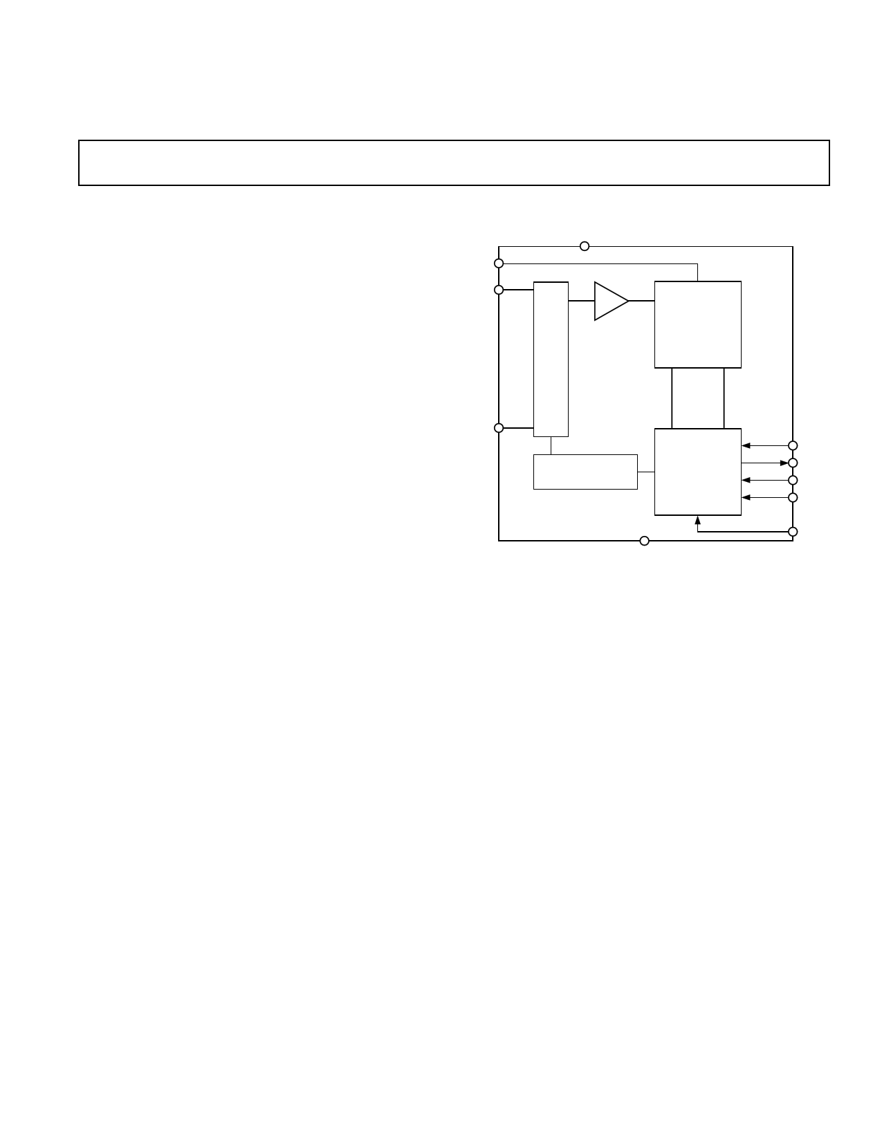
FUNCTIONAL BLOCK DIAGRAM
VDD
REFIN
VIN0
•
•
•
•
•
•
•
•
•
•
•
•
•
VIN3
T/H
I/P
MUX
8-/10-/12-BIT
SUCCESSIVE
APPROXIMATION
ADC
SEQUENCER
CONTROL LOGIC
AD7904/AD7914/AD7924
GND
SCLK
DOUT
DIN
CS
VDRIVE
PRODUCT HIGHLIGHTS
1. High Throughput with Low Power Consumption.
The AD7904/AD7914/AD7924 offer up to 1 MSPS through-
put rates. At the maximum throughput rate with 3 V sup`plies,
the AD7904/AD7914/AD7924 dissipate just 6 mW of
power maximum.
2. Four Single-Ended Inputs with a Channel Sequencer.
A consecutive sequence of channels can be selected, through
which the ADC will cycle and convert on.
3. Single-Supply Operation with VDRIVE Function.
The AD7904/AD7914/AD7924 operate from a single 2.7 V
to 5.25 V supply. The VDRIVE function allows the serial inter-
face to connect directly to either 3 V or 5 V processor systems
independent of VDD.
4. Flexible Power/Serial Clock Speed Management.
The conversion rate is determined by the serial clock, allowing
the conversion time to be reduced through the serial clock speed
increase. The parts also feature various shutdown modes to
maximize power efficiency at lower throughput rates. Current
consumption is 0.5 µA max when in full shutdown.
5. No Pipeline Delay.
The parts feature a standard successive-approximation ADC
with accurate control of the sampling instant via a CS input
and once off conversion control.
REV. 0
Information furnished by Analog Devices is believed to be accurate and
reliable. However, no responsibility is assumed by Analog Devices for its
use, nor for any infringements of patents or other rights of third parties that
may result from its use. No license is granted by implication or otherwise
under any patent or patent rights of Analog Devices.
One Technology Way, P.O. Box 9106, Norwood, MA 02062-9106, U.S.A.
Tel: 781/329-4700
www.analog.com
Fax: 781/326-8703
© Analog Devices, Inc., 2002
Free Datasheet http://www.datasheet4u.com/
1 page 
Parameter
B Version1
POWER REQUIREMENTS
VDD
VDRIVE
IDD4
Normal Mode (Static)
Normal Mode (Operational)
Using Auto Shutdown Mode
Full Shutdown Mode
Power Dissipation4
Normal Mode (Operational)
Auto Shutdown Mode (Static)
Full Shutdown Mode
2.7/5.25
2.7/5.25
600
2.7
2
960
0.5
0.5
13.5
6
2.5
1.5
2.5
1.5
NOTES
1Temperature ranges as follows: B Version: –40°C to +85°C.
2See Terminology section.
3Sample tested @ 25°C to ensure compliance.
4See Power Versus Throughput Rate section.
Specifications subject to change without notice.
AD7904/AD7914/AD7924
Unit
Test Conditions/Comments
V min/max
V min/max
µA typ
mA max
mA max
µA typ
µA max
µA max
Digital I/Ps = 0 V or VDRIVE
VDD = 2.7 V to 5.25 V, SCLK On or Off
VDD = 4.75 V to 5.25 V, fSCLK = 20 MHz
VDD = 2.7 V to 3.6 V, fSCLK = 20 MHz
fSAMPLE = 250 kSPS
(Static)
SCLK On or Off (20 nA typ)
mW max
mW max
µW max
µW max
µW max
µW max
VDD = 5 V, fSCLK = 20 MHz
VDD = 3 V, fSCLK = 20 MHz
VDD = 5 V
VDD = 3 V
VDD = 5 V
VDD = 3 V
REV. 0
–5–
Free Datasheet http://www.datasheet4u.com/
5 Page 
AD7904/AD7914/AD7924
TERMINOLOGY
Integral Nonlinearity
This is the maximum deviation from a straight line passing
through the endpoints of the ADC transfer function. The end-
points of the transfer function are zero scale, a point 1 LSB
below the first code transition, and full scale, a point 1 LSB
above the last code transition.
Differential Nonlinearity
This is the difference between the measured and the ideal 1 LSB
change between any two adjacent codes in the ADC.
Offset Error
This is the deviation of the first code transition (00 . . . 000) to
(00 . . . 001) from the ideal, i.e., AGND + 1 LSB.
Offset Error Match
This is the difference in offset error between any two channels.
Gain Error
This is the deviation of the last code transition (111 . . . 110) to
(111 . . . 111) from the ideal (i.e., REFIN – 1 LSB) after the
offset error has been adjusted out.
Gain Error Match
This is the difference in Gain error between any two channels.
Zero Code Error
This applies when using the twos complement output coding
option, in particular to the 2 × REFIN input range with –REFIN
to +REFIN biased about the REFIN point. It is the deviation of
the midscale transition (all 0s to all 1s) from the ideal VIN volt-
age, i.e., REFIN – 1 LSB.
Zero Code Error Match
This is the difference in Zero Code Error between any two
channels.
Positive Gain Error
This applies when using the twos complement output coding
option, in particular to the 2 × REFIN input range with –REFIN
to +REFIN biased about the REFIN point. It is the deviation of
the last code transition (011. . .110) to (011 . . . 111) from the
ideal (i.e., +REFIN – 1 LSB) after the Zero Code Error has been
adjusted out.
Positive Gain Error Match
This is the difference in Positive Gain Error between any two
channels.
Negative Gain Error
This applies when using the twos complement output coding
option, in particular to the 2 × REFIN input range with –REF IN
to +REFIN biased about the REFIN point. It is the deviation of
the first code transition (100 . . . 000) to (100 . . . 001) from the
ideal (i.e., –REF IN + 1 LSB) after the Zero Code Error has
been adjusted out.
Negative Gain Error Match
This is the difference in Negative Gain Error between any two
channels.
Channel-to-Channel Isolation
Channel-to-Channel Isolation is a measure of the level of crosstalk
between channels. It is measured by applying a full-scale 400 kHz
sine wave signal to all three nonselected input channels and deter-
mining how much that signal is attenuated in the selected channel
with a 50 kHz signal. The figure is given worst case across all
four channels for the AD7904/AD7914/AD7924.
PSR (Power Supply Rejection)
Variations in power supply will affect the full scale transition,
but not the converter’s linearity. Power supply rejection is the
maximum change in full-scale transition point due to a change
in power-supply voltage from the nominal value. See Typical
Performance Curves.
Track/Hold Acquisition Time
The track/hold amplifier returns into track mode at the end
of conversion. Track/Hold acquisition time is the time required
for the output of the track/hold amplifier to reach its final
value, within ± 1 LSB, after the end of conversion.
Signal to (Noise + Distortion) Ratio
This is the measured ratio of signal to (noise + distortion) at the
output of the A/D converter. The signal is the rms amplitude of
the fundamental. Noise is the sum of all nonfundamental sig-
nals up to half the sampling frequency (fS/2), excluding dc. The
ratio is dependent on the number of quantization levels in the
digitization process; the more levels, the smaller the quantiza-
tion noise. The theoretical signal to (noise + distortion) ratio for
an ideal N-bit converter with a sine wave input is given by:
Signal to(Noise + Distortion) = (6.02N + 1.76)dB
Thus for a 12-bit converter, this is 74 dB, for a 10-bit converter
this is 62 dB, and for an 8-bit converter this is 50 dB.
Total Harmonic Distortion
Total harmonic distortion (THD) is the ratio of the rms sum of
harmonics to the fundamental. For the AD7904/AD7914/AD7924, it
is defined as:
THD(dB) = 20 log V22 +V32 +V42 +V52 +V62
V1
where V1 is the rms amplitude of the fundamental and V2, V3,
V4, V5, and V6 are the rms amplitudes of the second through the
sixth harmonics.
REV. 0
–11–
Free Datasheet http://www.datasheet4u.com/
11 Page | ||
| Páginas | Total 24 Páginas | |
| PDF Descargar | [ Datasheet AD7914.PDF ] | |
Hoja de datos destacado
| Número de pieza | Descripción | Fabricantes |
| AD7910 | 10-/12-Bit ADCs | Analog Devices |
| AD7911 | 10-/12-Bit ADCs | Analog Devices |
| AD7912 | 2-Channel/ 2.35 V to 5.25 V/ 1 MSPS/ 10-/12-Bit ADCs | Analog Devices |
| AD7914 | (AD79x4) 8-/10-/12-Bit ADCs | Analog Devices |
| Número de pieza | Descripción | Fabricantes |
| SLA6805M | High Voltage 3 phase Motor Driver IC. |
Sanken |
| SDC1742 | 12- and 14-Bit Hybrid Synchro / Resolver-to-Digital Converters. |
Analog Devices |
|
DataSheet.es es una pagina web que funciona como un repositorio de manuales o hoja de datos de muchos de los productos más populares, |
| DataSheet.es | 2020 | Privacy Policy | Contacto | Buscar |