|
|
|
PDF ACT8937A Data sheet ( Hoja de datos )
| Número de pieza | ACT8937A | |
| Descripción | Advanced PMU | |
| Fabricantes | Active-Semi | |
| Logotipo | ||
Hay una vista previa y un enlace de descarga de ACT8937A (archivo pdf) en la parte inferior de esta página. Total 30 Páginas | ||
|
No Preview Available !
ACT8937A
Rev 1, 22-Oct-12
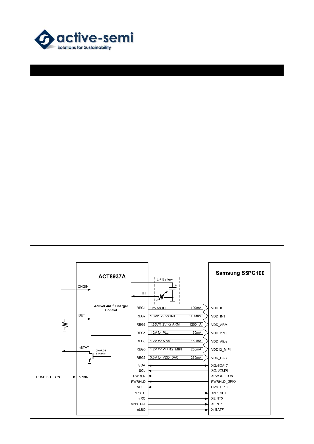
Advanced PMU for Samsung S5PC100, S5PC110 and S5PV210 Processors
FEATURES
• Optimized for Samsung S5PC100, S5PC110 and
S5PV210 Processors
• Three Step-Down DC/DC Converters
• Four Low-Dropout Linear Regulators
• Integrated ActivePathTM Charger
• I2CTM Serial Interface
• Advanced Enable/Disable Sequencing Controller
• Minimal External Components
• Tiny 5×5mm TQFN55-40 Package
− 0.75mm Package Height
− Pb-Free and RoHS Compliant
GENERAL DESCRIPTION
The ACT8937A is a complete, cost effective, highly-
efficient ActivePMUTM power management solution,
optimized for the unique power, voltage-
sequencing, and control requirements of the
Samsung S5PC100, S5PC110 and S5PV210
processors.
This device features three step-down DC/DC
converters and four low-noise, low-dropout linear
regulators, along with a complete battery charging
solution featuring the advanced ActivePathTM
system-power selection function.
The three DC/DC converters utilize a high-
efficiency, fixed-frequency (2MHz), current-mode
PWM control architecture that requires a minimum
number of external components. Two DC/DCs are
capable of supplying up to 1100mA of output
current, while the third supports up to 1200mA. All
four low-dropout linear regulators are high-
performance, low-noise regulators that supply up to
150mA, 150mA, 250mA, and 250mA, respectively.
The ACT8937A is available in a compact, Pb-Free
and RoHS-compliant TQFN55-40 package.
TYPICAL APPLICATION DIAGRAM
Innovative PowerTM
ActivePMUTM and ActivePathTM are trademarks of Active-Semi.
I2CTM is a trademark of NXP.
-1-
www.active-semi.com
Copyright © 2012 Active-Semi, Inc.
Free Datasheet http://www.datasheet4u.com/
1 page 
ACT8937A
Rev 1, 22-Oct-12
PIN DESCRIPTIONS
PIN NAME
DESCRIPTION
1
REFBP
Reference Bypass. Connect a 0.047μF ceramic capacitor from REFBP to GA. This pin is
discharged to GA in shutdown.
2 OUT1 Output Feedback Sense for REG1.
3
GA
Analog Ground. Connect GA directly to a quiet ground node. Connect GA, GP12 and GP3
together at a single point as close to the IC as possible.
4
OUT4
REG4 output. Capable of delivering up to 150mA of output current. Connect a 1.5µF ceramic
capacitor from OUT4 to GA. The output is discharged to GA with 1.5kΩ resistor when disabled.
5
OUT5
REG5 output. Capable of delivering up to 150mA of output current. Connect a 1.5µF ceramic
capacitor from OUT5 to GA. The output is discharged to GA with 1.5kΩ resistor when disabled.
6
INL
Power Input for REG4, REG5, REG6, and REG7. Bypass to GA with a high quality ceramic
capacitor placed as close to the IC as possible.
7
OUT7
REG7 output. Capable of delivering up to 250mA of output current. Connect a 2.2µF ceramic
capacitor from OUT7 to GA. The output is discharged to GA with 1.5kΩ resistor when disabled.
8
OUT6
REG6 output. Capable of delivering up to 250mA of output current. Connect a 2.2µF ceramic
capacitor from OUT6 to GA. The output is discharged to GA with 1.5kΩ resistor when disabled.
Master Enable Input. Drive nPBIN to GA through a 50kΩ resistor to enable the IC, drive nPBIN
9 nPBIN directly to GA to assert a manual reset condition. Refer to the nPBIN Multi-Function Input section
for more information. nPBIN is internally pulled up to VSYS through a 35kΩ resistor.
10
PWRHLD
Power Hold Input. PWRHLD is internally pulled down to GA with a 500kΩ resistor. Refer to the
Control Sequences section for more information.
11 nRSTO Active Low Reset Output. See the nRSTO Output section for more information.
12
nIRQ
Open-Drain Interrupt Output. nIRQ is asserted any time an unmasked fault condition exists or a
charger interrupt occurs. See the nIRQ Output section for more information.
13
nPBSTAT
Active-Low Open-Drain Push-Button Status Output. nPBSTAT is asserted low whenever the
nPBIN is pushed, and is high-Z otherwise. See the nPBSTAT Output section for more information.
14
GP3
Power Ground for REG3. Connect GA, GP12, and GP3 together at a single point as close to the
IC as possible.
15 SW3 Switching Node Output for REG3.
16
VP3
Power Input for REG3. Bypass to GP3 with a high quality ceramic capacitor placed as close to the
IC as possible.
17 OUT3 Output Feedback Sense for REG3.
18 PWREN Power Enable Input. Refer to the Control Sequences section for more information.
19
nLBO
Low Battery Indicator Output. nLBO is asserted low whenever the voltage at LBI is lower than
1.2V, and is high-Z otherwise. See the Precision Voltage Detector section for more information.
20
LBI
Low Battery Input. The input voltage is compared to 1.2V and the output of this comparison drives
nLBO. See the Precision Voltage Detector section for more information.
21 ACIN AC Input Supply Detection. See the Charge Current Programming section for more information.
22 CHGLEV Charge Current Selection Input. See the Charge Current Programming section for more information.
Innovative PowerTM
ActivePMUTM and ActivePathTM are trademarks of Active-Semi.
I2CTM is a trademark of NXP.
-5-
www.active-semi.com
Copyright © 2012 Active-Semi, Inc.
Free Datasheet http://www.datasheet4u.com/
5 Page 
REGISTER AND BIT DESCRIPTIONS CONT’D
ACT8937A
Rev 1, 22-Oct-12
OUTPUT ADDRESS BIT NAME ACCESS
DESCRIPTION
REG2
REG2
0x31 [5:0] VSET2
0x32
[7]
ON
Secondary Output Voltage Selection. Valid when VSEL is
R/W driven high. See the Output Voltage Programming section for
more information.
R/W
Regulator Enable Bit. Set bit to 1 to enable the regulator, clear
bit to 0 to disable the regulator.
REG2
0x32
[6] PHASE
Regulator Phase Control. Set bit to 1 for the regulator to
R/W operate 180° out of phase with the oscillator, clear bit to 0 for
the regulator to operate in phase with the oscillator.
REG2
REG2
REG2
REG2
REG3
0x32
0x32
0x32
0x32
0x40
[5] MODE
[4:2] DELAY
[1] nFLTMSK
[0] OK
[7:6] -
Regulator Mode Select. Set bit to 1 for fixed-frequency PWM
R/W under all load conditions, clear bit to 0 to transit to power-
savings mode under light-load conditions.
R/W
Regulator Turn-On Delay Control. See the REG1, REG2,
REG3 Turn-on Delay section for more information.
R/W
Regulator Fault Mask Control. Set bit to 1 enable fault-
interrupts, clear bit to 0 to disable fault-interrupts.
R
Regulator Power-OK Status. Value is 1 when output voltage
exceeds the power-OK threshold, value is 0 otherwise.
R Reserved.
REG3
0x40 [5:0] VSET1
Primary Output Voltage Selection. Valid when VSEL is driven
R/W low. See the Output Voltage Programming section for more
information.
REG3
0x41 [7:6]
-
R Reserved.
REG3
0x41 [5:0] VSET2
Secondary Output Voltage Selection. Valid when VSEL is
R/W driven high. See the Output Voltage Programming section for
more information.
REG3
0x42
[7]
ON
R/W
Regulator Enable Bit. Set bit to 1 to enable the regulator, clear
bit to 0 to disable the regulator.
REG3
0x42
[6]
-
R/W Reserved.
REG3
REG3
REG3
REG3
REG4
REG4
REG4
REG4
REG4
REG4
REG4
0x42
0x42
0x42
0x42
0x50
0x50
0x51
0x51
0x51
0x51
0x51
[5] MODE
[4:2] DELAY
[1] nFLTMSK
[0] OK
[7:6] -
[5:0] VSET
[7] ON
[6] DIS
[5] LOWIQ
[4:2] DELAY
[1] nFLTMSK
Regulator Mode Select. Set bit to 1 for fixed-frequency PWM
R/W under all load conditions, clear bit to 0 to transit to power-
savings mode under light-load conditions.
R/W
Regulator Turn-On Delay Control. See the REG1, REG2,
REG3 Turn-on Delay section for more information.
R/W
Regulator Fault Mask Control. Set bit to 1 enable fault-
interrupts, clear bit to 0 to disable fault-interrupts.
R
Regulator Power-OK Status. Value is 1 when output voltage
exceeds the power-OK threshold, value is 0 otherwise.
R Reserved.
R/W
Output Voltage Selection. See the Output Voltage
Programming section for more information.
R/W
Regulator Enable Bit. Set bit to 1 to enable the regulator, clear
bit to 0 to disable the regulator.
Output Discharge Control. When activated, LDO output is
R/W
discharged to GA through 1.5kΩ resistor when in shutdown.
Set bit to 1 to enable output voltage discharge in shutdown,
clear bit to 0 to disable this function.
R/W
LDO Low-IQ Mode Control. Set bit to 1 for low-power
operating mode, clear bit to 0 for normal mode.
R/W
Regulator Turn-On Delay Control. See the REG4, REG5,
REG6, REG7 Turn-on Delay section for more information.
R/W
Regulator Fault Mask Control. Set bit to 1 enable fault-
interrupts, clear bit to 0 to disable fault-interrupts.
Innovative PowerTM
ActivePMUTM and ActivePathTM are trademarks of Active-Semi.
I2CTM is a trademark of NXP.
- 11 -
www.active-semi.com
Copyright © 2012 Active-Semi, Inc.
Free Datasheet http://www.datasheet4u.com/
11 Page | ||
| Páginas | Total 30 Páginas | |
| PDF Descargar | [ Datasheet ACT8937A.PDF ] | |
Hoja de datos destacado
| Número de pieza | Descripción | Fabricantes |
| ACT8937 | Advanced PMU | Active-Semi |
| ACT8937A | Advanced PMU | Active-Semi |
| Número de pieza | Descripción | Fabricantes |
| SLA6805M | High Voltage 3 phase Motor Driver IC. |
Sanken |
| SDC1742 | 12- and 14-Bit Hybrid Synchro / Resolver-to-Digital Converters. |
Analog Devices |
|
DataSheet.es es una pagina web que funciona como un repositorio de manuales o hoja de datos de muchos de los productos más populares, |
| DataSheet.es | 2020 | Privacy Policy | Contacto | Buscar |