|
|
|
PDF ADSP-BF607 Data sheet ( Hoja de datos )
| Número de pieza | ADSP-BF607 | |
| Descripción | (ADSP-BF606 - ADSP-BF609) Blackfin Dual Core Embedded Processor | |
| Fabricantes | Analog Devices | |
| Logotipo | ||
Hay una vista previa y un enlace de descarga de ADSP-BF607 (archivo pdf) en la parte inferior de esta página. Total 30 Páginas | ||
|
No Preview Available !
Blackfin Dual Core
Embedded Processor
ADSP-BF606/ADSP-BF607/ADSP-BF608/ADSP-BF609
FEATURES
Dual-core symmetric high-performance Blackfin processor,
up to 500 MHz per core
Each core contains two 16-bit MACs, two 40-bit ALUs, and a
40-bit barrel shifter
RISC-like register and instruction model for ease of
programming and compiler-friendly support
Advanced debug, trace, and performance monitoring
Pipelined Vision Processor provides hardware to process sig-
nal and image algorithms used for pre- and co-processing
of video frames in ADAS or other video processing
applications
Accepts a range of supply voltages for I/O operation. See
Operating Conditions on Page 52
Off-chip voltage regulator interface
349-ball BGA package (19 mm × 19 mm), RoHS compliant
MEMORY
Each core contains 148K bytes of L1 SRAM memory (proces-
sor core-accessible) with multi-parity bit protection
Up to 256K bytes of L2 SRAM memory with ECC protection
Dynamic memory controller provides 16-bit interface to a
single bank of DDR2 or LPDDR DRAM devices
Static memory controller with asynchronous memory inter-
face that supports 8-bit and 16-bit memories
4 Memory-to-memory DMA streams, 2 of which feature CRC
protection
Flexible booting options from flash, SD EMMC and SPI mem-
ories and from SPI, link port and UART hosts
Memory management unit provides memory protection
EMULATOR
TEST & CONTROL
PLL & POWER
MANAGEMENT
FAULT
MANAGEMENT
SYSTEM CONTROL BLOCKS
EVENT
CONTROL
DUAL
WATCHDOG
PERIPHERALS
2× TWI
8× TIMER
CORE 0
B
148K BYTE
PARITY BIT PROTECTED
L1 SRAM
INSTRUCTION/DATA
CORE 1
B
148K BYTE
PARITY BIT PROTECTED
L1 SRAM
INSTRUCTION/DATA
L2 MEMORY
32K BYTE
ROM
256K BYTE
ECC-
PROTECTED
SRAM
1× COUNTER
2× PWM
3× SPORT
1× ACM
2× UART
EMMC/RSI
112
GP
I/O
DMA SYSTEM
EXTERNAL
BUS
INTERFACES
DYNAMIC
MEMORY
CONTROLLER
STATIC
MEMORY
CONTROLLER
LPDDR
DDR2
16
FLASH
SRAM
16
CRC
HARDWARE
FUNCTIONS
PIPELINED
VISION PROCESSOR
VIDEO
SUBSYSTEM
PIXEL
COMPOSITOR
1× CAN
2× EMAC
WITH
2× IEEE 1588
2× SPI
4× LINK PORT
3× PPI
USB 2.0 HS OTG
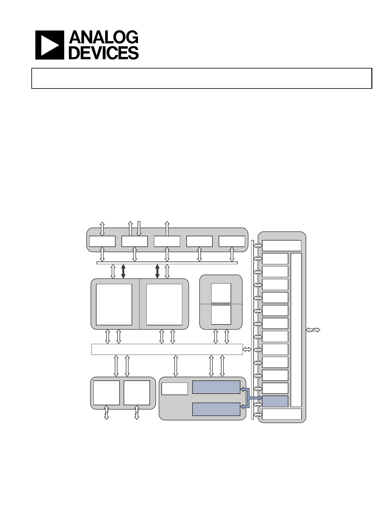
Figure 1. Processor Block Diagram
Blackfin and the Blackfin logo are registered trademarks of Analog Devices, Inc.
Rev. 0
Document Feedback
Information furnished by Analog Devices is believed to be accurate and reliable.
However, no responsibility is assumed by Analog Devices for its use, nor for any
infringements of patents or other rights of third parties that may result from its use.
Specifications subject to change without notice. No license is granted by implication
or otherwise under any patent or patent rights of Analog Devices. Trademarks and
registered trademarks are the property of their respective owners.
One Technology Way, P.O. Box 9106, Norwood, MA 02062-9106 U.S.A.
Tel: 781.329.4700
©2013 Analog Devices, Inc. All rights reserved.
Technical Support
www.analog.com
Free Datasheet http://www.datasheet4u.com/
1 page 
ADSP-BF606/ADSP-BF607/ADSP-BF608/ADSP-BF609
a very small final memory size. The instruction set also provides
fully featured multifunction instructions that allow the pro-
grammer to use many of the processor core resources in a single
instruction. Coupled with many features more often seen on
microcontrollers, this instruction set is very efficient when com-
piling C and C++ source code. In addition, the architecture
supports both user (algorithm/application code) and supervisor
(O/S kernel, device drivers, debuggers, ISRs) modes of opera-
tion, allowing multiple levels of access to core
processor resources.
The assembly language, which takes advantage of the proces-
sor’s unique architecture, offers the following advantages:
• Seamlessly integrated DSP/MCU features are optimized for
both 8-bit and 16-bit operations.
• A multi-issue load/store modified-Harvard architecture,
which supports two 16-bit MAC or four 8-bit ALU + two
load/store + two pointer updates per cycle.
• All registers, I/O, and memory are mapped into a unified
4G byte memory space, providing a simplified program-
ming model.
• Control of all asynchronous and synchronous events to the
processor is handled by two subsystems: the Core Event
Controller (CEC) and the System Event Controller (SEC).
• Microcontroller features, such as arbitrary bit and bit-field
manipulation, insertion, and extraction; integer operations
on 8-, 16-, and 32-bit data-types; and separate user and
supervisor stack pointers.
• Code density enhancements, which include intermixing of
16-bit and 32-bit instructions (no mode switching, no code
segregation). Frequently used instructions are encoded
in 16 bits.
PROCESSOR INFRASTRUCTURE
The following sections provide information on the primary
infrastructure components of the ADSP-BF609 processor.
DMA Controllers
The processor uses Direct Memory Access (DMA) to transfer
data within memory spaces or between a memory space and a
peripheral. The processor can specify data transfer operations
and return to normal processing while the fully integrated DMA
controller carries out the data transfers independent of proces-
sor activity.
DMA transfers can occur between memory and a peripheral or
between one memory and another memory. Each Memory-to-
memory DMA stream uses two channels, where one channel is
the source channel, and the second is the destination channel.
All DMAs can transport data to and from all on-chip and off-
chip memories. Programs can use two types of DMA transfers,
descriptor-based or register-based. Register-based DMA allows
the processor to directly program DMA control registers to ini-
tiate a DMA transfer. On completion, the control registers may
be automatically updated with their original setup values for
continuous transfer. Descriptor-based DMA transfers require a
set of parameters stored within memory to initiate a DMA
sequence. Descriptor-based DMA transfers allow multiple
DMA sequences to be chained together and a DMA channel can
be programmed to automatically set up and start another DMA
transfer after the current sequence completes.
The DMA controller supports the following DMA operations.
• A single linear buffer that stops on completion.
• A linear buffer with negative, positive or zero stride length.
• A circular, auto-refreshing buffer that interrupts when each
buffer becomes full.
• A similar buffer that interrupts on fractional buffers (for
example, 1/2, 1/4).
• 1D DMA – uses a set of identical ping-pong buffers defined
by a linked ring of two-word descriptor sets, each contain-
ing a link pointer and an address.
• 1D DMA – uses a linked list of 4 word descriptor sets con-
taining a link pointer, an address, a length, and a
configuration.
• 2D DMA – uses an array of one-word descriptor sets, spec-
ifying only the base DMA address.
• 2D DMA – uses a linked list of multi-word descriptor sets,
specifying everything.
CRC Protection
The two CRC protection modules allow system software to peri-
odically calculate the signature of code and/or data in memory,
the content of memory-mapped registers, or communication
message objects. Dedicated hardware circuitry compares the
signature with pre calculated values and triggers appropriate
fault events.
For example, every 100 ms the system software might initiate
the signature calculation of the entire memory contents and
compare these contents with expected, pre calculated values. If a
mismatch occurs, a fault condition can be generated (via the
processor core or the trigger routing unit).
The CRC is a hardware module based on a CRC32 engine that
computes the CRC value of the 32-bit data words presented to
it. Data is provided by the source channel of the memory-to-
memory DMA (in memory scan mode) and is optionally for-
warded to the destination channel (memory transfer mode).
The main features of the CRC peripheral are:
• Memory scan mode
• Memory transfer mode
• Data verify mode
• Data fill mode
• User-programmable CRC32 polynomial
• Bit/byte mirroring option (endianness)
• Fault/error interrupt mechanisms
• 1D and 2D fill block to initialize array with constants.
• 32-bit CRC signature of a block of a memory or MMR
block.
Rev. 0 | Page 5 of 112 | June 2013
Free Datasheet http://www.datasheet4u.com/
5 Page 
ADSP-BF606/ADSP-BF607/ADSP-BF608/ADSP-BF609
Memory Protection
The Blackfin cores feature a memory protection concept, which
grants data and/or instruction accesses from enabled memory
regions only. A supervisor mode vs. user mode programming
model supports dynamically varying access rights. Increased
flexibility in memory page size options supports a simple
method of static memory partitioning.
System Protection
All system resources and L2 memory banks can be controlled by
either the processor cores, memory-to-memory DMA, or the
system debug unit (SDU). A system protection unit (SPU)
enables write accesses to specific resources that are locked to
any of four masters: Core 0, Core 1, Memory DMA, and the Sys-
tem Debug Unit. System protection is enabled in greater
granularity for some modules (L2, SEC and GPIO controllers)
through a global lock concept.
Watchpoint Protection
The primary purpose of watchpoints and hardware breakpoints
is to serve emulator needs. When enabled, they signal an emula-
tor event whenever user-defined system resources are accessed
or a core executes from user-defined addresses. Watchdog
events can be configured such that they signal the events to the
other Blackfin core or to the fault management unit.
Dual Watchdog
The two on-chip watchdog timers each may supervise one
Blackfin core.
Bandwidth Monitor
All DMA channels that operate in memory-to-memory mode
(Memory DMA, PVP Memory Pipe DMA, PIXC DMA) are
equipped with a bandwidth monitor mechanism. They can sig-
nal a system event or fault when transactions tend to starve
because system buses are fully loaded with higher-priority
traffic.
Signal Watchdogs
The eight general-purpose timers feature two new modes to
monitor off-chip signals. The Watchdog Period mode monitors
whether external signals toggle with a period within an expected
range. The Watchdog Width mode monitors whether the pulse
widths of external signals are in an expected range. Both modes
help to detect incorrect undesired toggling (or lack thereof) of
system-level signals.
Up/Down Count Mismatch Detection
The up/down counter can monitor external signal pairs, such as
request/grant strobes. If the edge count mismatch exceeds the
expected range, the up/down counter can flag this to the proces-
sor or to the fault management unit.
Fault Management
The fault management unit is part of the system event controller
(SEC). Any system event, whether a dual-bit uncorrectable ECC
error, or any peripheral status interrupt, can be defined as being
a “fault”. Additionally, the system events can be defined as an
interrupt to the cores. If defined as such, the SEC forwards the
event to the fault management unit which may automatically
reset the entire device for reboot, or simply toggle the SYS_
FAULT output pins to signal off-chip hardware. Optionally, the
fault management unit can delay the action taken via a keyed
sequence, to provide a final chance for the Blackfin cores to
resolve the crisis and to prevent the fault action from being
taken.
ADDITIONAL PROCESSOR PERIPHERALS
The processor contains a rich set of peripherals connected to the
core via several high-bandwidth buses, providing flexibility in
system configuration as well as excellent overall system perfor-
mance (see the block diagram on Page 1). The processors
contain high-speed serial and parallel ports, an interrupt con-
troller for flexible management of interrupts from the on-chip
peripherals or external sources, and power management control
functions to tailor the performance and power characteristics of
the processor and system to many application scenarios.
The following sections describe additional peripherals that were
not described in the previous sections.
Timers
The processor includes several timers which are described in the
following sections.
General-Purpose Timers
There is one GP timer unit and it provides eight general-pur-
pose programmable timers. Each timer has an external pin that
can be configured either as a pulse width modulator (PWM) or
timer output, as an input to clock the timer, or as a mechanism
for measuring pulse widths and periods of external events.
These timers can be synchronized to an external clock input on
the TMRx pins, an external clock TMRCLK input pin, or to the
internal SCLK0.
The timer units can be used in conjunction with the UARTs and
the CAN controller to measure the width of the pulses in the
data stream to provide a software auto-baud detect function for
the respective serial channels.
The timers can generate interrupts to the processor core, pro-
viding periodic events for synchronization to either the system
clock or to external signals. Timer events can also trigger other
peripherals via the TRU (for instance, to signal a fault).
Core Timers
Each processor core also has its own dedicated timer. This extra
timer is clocked by the internal processor clock and is typically
used as a system tick clock for generating periodic operating
system interrupts.
Watchdog Timers
Each core includes a 32-bit timer, which may be used to imple-
ment a software watchdog function. A software watchdog can
improve system availability by forcing the processor to a known
state, via generation of a hardware reset, nonmaskable interrupt
(NMI), or general-purpose interrupt, if the timer expires before
Rev. 0 | Page 11 of 112 | June 2013
Free Datasheet http://www.datasheet4u.com/
11 Page | ||
| Páginas | Total 30 Páginas | |
| PDF Descargar | [ Datasheet ADSP-BF607.PDF ] | |
Hoja de datos destacado
| Número de pieza | Descripción | Fabricantes |
| ADSP-BF606 | (ADSP-BF606 - ADSP-BF609) Blackfin Dual Core Embedded Processor | Analog Devices |
| ADSP-BF607 | (ADSP-BF606 - ADSP-BF609) Blackfin Dual Core Embedded Processor | Analog Devices |
| ADSP-BF608 | (ADSP-BF606 - ADSP-BF609) Blackfin Dual Core Embedded Processor | Analog Devices |
| ADSP-BF609 | (ADSP-BF606 - ADSP-BF609) Blackfin Dual Core Embedded Processor | Analog Devices |
| Número de pieza | Descripción | Fabricantes |
| SLA6805M | High Voltage 3 phase Motor Driver IC. |
Sanken |
| SDC1742 | 12- and 14-Bit Hybrid Synchro / Resolver-to-Digital Converters. |
Analog Devices |
|
DataSheet.es es una pagina web que funciona como un repositorio de manuales o hoja de datos de muchos de los productos más populares, |
| DataSheet.es | 2020 | Privacy Policy | Contacto | Buscar |