|
|
|
PDF ADM13305 Data sheet ( Hoja de datos )
| Número de pieza | ADM13305 | |
| Descripción | Dual Processor Supervisors | |
| Fabricantes | Analog Devices | |
| Logotipo | ||
Hay una vista previa y un enlace de descarga de ADM13305 (archivo pdf) en la parte inferior de esta página. Total 12 Páginas | ||
|
No Preview Available !
FEATURES
Dual supervisory circuits
Supply voltage range of 2.7 V to 5.5 V
Pretrimmed threshold options: 1.8 V, 2.5 V, 3.3 V, and 5 V
Adjustable 0.6 V voltage reference
Maximum supply current of 40 μA
140 ms (minimum) reset timeout
Watchdog timer with 1.6 sec (typical) timeout
RESET valid from VDD ≥ 1.1 V
Push-pull RESET and RESET outputs
8-lead, narrow body SOIC package
Temperature range: −40°C to +85°C
APPLICATIONS
Supervising DSPs/microcontrollers
Industrial and portable equipment
Wireless systems
Notebook/desktop computers
GENERAL DESCRIPTION
The ADM13305 is a dual voltage supervisor designed to
monitor two supplies and provide a reset signal to DSP and
microprocessor-based systems.
There are five models available, all of which feature a combination
of internally pretrimmed undervoltage threshold options for
monitoring 1.8 V, 2.5 V, 3.3 V, and 5 V supplies. There is also
an adjustable input option with an undervoltage threshold voltage
of 0.6 V.
The ADM13305-18, ADM13305-25, and ADM13305-33 models
have two internally fixed thresholds. The ADM13305-4 and
ADM13305-5 offer one internally fixed threshold and one
externally programmable threshold via a resistor string. See
the Ordering Guide for a list of all available options.
During power-up, RESET is asserted when the supply voltage
exceeds 1.1 V. The device then monitors the SENSEv input pins
and holds the RESET output low as long as either of the SENSEv
inputs remains below the rising threshold voltage, VIT+.
Once the supplies monitored at the SENSEv inputs rise above
their associated thresholds, the reset signal remains low for
the reset timeout period before deasserting. Subsequently, if a
voltage monitored by the SENSEv pins falls below its associ-
ated falling threshold, VIT−, the RESET output asserts. The
ADM13305 features both an active high RESET and an active
low RESET output.
Rev. 0
Information furnished by Analog Devices is believed to be accurate and reliable. However, no
responsibility is assumed by Analog Devices for its use, nor for any infringements of patents or other
rights of third parties that may result from its use. Specifications subject to change without notice. No
license is granted by implication or otherwise under any patent or patent rights of Analog Devices.
Trademarksandregisteredtrademarksarethepropertyoftheirrespectiveowners.
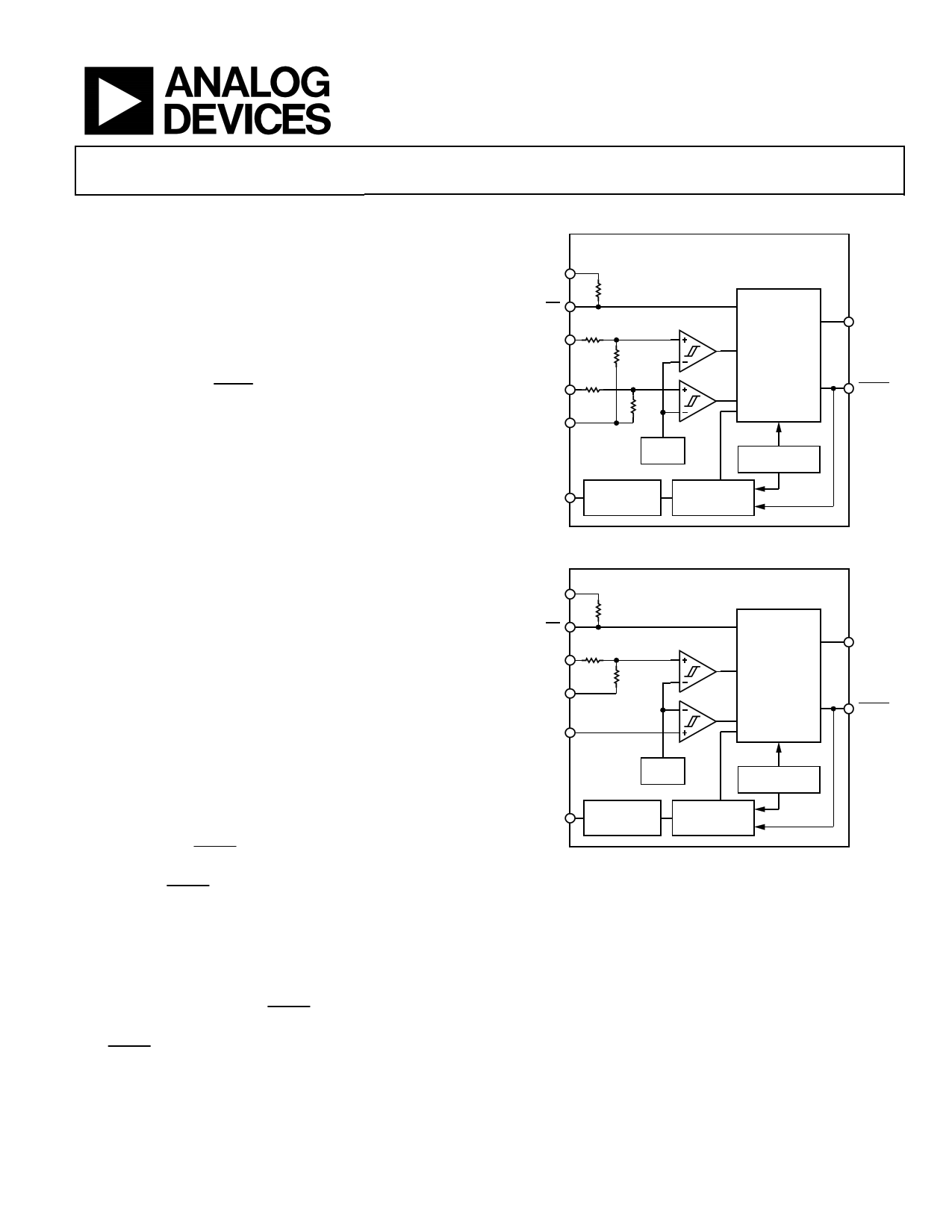
Dual Processor
Supervisors with Watchdog
ADM13305
VDD
MR
SENSE1
SENSE2
GND
FUNCTIONAL BLOCK DIAGRAMS
ADM13305-18
ADM13305-25
ADM13305-33
14kΩ
R1 R2
RESET
LOGIC + TIMER
RESET
R3 R4
RESET
1.25V
OSCILLATOR
WDI
TRANSITION
DETECTION
WATCHDOG
LOGIC + TIMER
Figure 1.
VDD
MR
SENSE1
GND
14kΩ
R1 R2
SENSE2
ADM13305-4
ADM13305-5
RESET
LOGIC + TIMER
RESET
RESET
WDI
0.6V
OSCILLATOR
TRANSITION
DETECTION
WATCHDOG
LOGIC + TIMER
Figure 2. .
As well as providing power-on reset signals, an on-chip watchdog
timer can reset the microprocessor if it fails to strobe within the
preset timeout period. A reset signal can also be asserted by an
external push button through the manual reset input pin.
The ADM13305 is available in an 8-lead, narrow body SOIC
package. The device operates over the extended industrial
temperature range of −40°C to +85°C.
One Technology Way, P.O. Box 9106, Norwood, MA 02062-9106, U.S.A.
Tel: 781.329.4700
www.analog.com
Fax: 781.461.3113
©2007 Analog Devices, Inc. All rights reserved.
Free Datasheet http://www.datasheet4u.com/
1 page 
ADM13305
TIMING REQUIREMENTS
VDD = 2.7 V to 5.5 V, RL = 1 MΩ, CL = 50 pF, TA = 25°C.
Table 3. ADM13305-18, ADM13305-25 and ADM13305-33
Parameter
Min Typ Max
PULSE WIDTH (tw)
SENSEv
6
MR 100
WDI 100
Unit
μs
ns
ns
Test Conditions/Comments
VSENSEvL = VIT− − 0.3 V, VSENSEvH = VIT+ + 0.3 V
VIH = 0.7 × VDD, VIL = 0.3 × VDD
VIH = 0.7 × VDD, VIL = 0.3 × VDD
Table 4. ADM13305-4 and ADM13305-5
Parameter
Min Typ Max Unit
PULSE WIDTH (tw)
SENSEv
30 μs
MR 100
ns
WDI 100
ns
Test Conditions/Comments
VSENSEvL = VIT− − 0.3 V, VSENSEvH = VIT+ + 0.3 V
VIH = 0.7 × VDD, VIL = 0.3 × VDD
VIH = 0.7 × VDD, VIL = 0.3 × VDD
SWITCHING CHARACTERISTICS
VDD = 2.7 V to 5.5 V, RL = 1 MΩ, CL = 50 pF, TA = 25°C.
Table 5. ADM13305-18, ADM13305-25 and ADM13305-33
Parameter
Min Typ Max Unit Test Conditions/Comments
Watchdog Timeout (tt(OUT))
1.1 1.6 2.3 sec VI(SENSEv) ≥ VIT+ + 0.2 V, MR ≥ 0.7 × VDD
Delay Time (td)
140 200 280 ms VI(SENSEv) ≥ VIT+ + 0.2 V, MR ≥ 0.7 × VDD
Propagation Delay, High-to-Low, MR to RESET1/RESET (tPHL)
200 500 ns
VI(SENSEv) ≥ VIT+ + 0.2 V, VIH ≥ 0.7 × VDD, VIL ≥ 0.3 × VDD
Propagation Delay, Low-to-High, MR to RESET/RESET1 (tPLH)
200 500 ns
VI(SENSEv) ≥ VIT+ + 0.2 V, VIH ≥ 0.7 × VDD, VIL ≥ 0.3 × VDD
Propagation Delay, High-to-Low, SENSEv to RESET1/RESET (tPHL)
15
μs VIH = VIT+ + 0.3 V, VIL = VIT− − 0.3 V, MR ≥ 0.7 × VDD
Propagation Delay, Low-to-High, SENSEv to RESET/RESET1 (tPLH)
15
μs VIH = VIT+ + 0.3 V, VIL = VIT− − 0.3 V, MR ≥ 0.7 × VDD
1 The reset timeout delay of 200 ms masks the propagation delay.
Table 6. ADM13305-4 and ADM13305-5
Parameter
Watchdog Timeout (tt(out))
Delay Time (td)
Propagation Delay, High-to-Low, MR to RESET1/RESET (tPHL)
Propagation Delay, Low-to-High, MR to RESET/RESET1 (tPLH)
Propagation Delay, High-to-Low, SENSEv to RESET1/RESET (tPHL)
Propagation Delay, Low-to-High, SENSEv to RESET/RESET1 (tPLH)
Min Typ Max Unit Test Conditions/Comments
1.1 1.6 2.3 sec VI(SENSEv) ≥ VIT+ + 0.2 V, MR ≥ 0.7 × VDD
140 200 280 ms VI(SENSEv) ≥ VIT+ + 0.2 V, MR ≥ 0.7 × VDD
200 500 ns
VI(SENSEv) ≥ VIT+ + 0.2 V, VIH ≥ 0.7 × VDD, VIL ≥ 0.3 × VDD
200 500 ns
VI(SENSEv) ≥ VIT+ + 0.2 V, VIH ≥ 0.7 × VDD, VIL ≥ 0.3 × VDD
30 μs VIH = VIT+ + 0.3 V, VIL = VIT− − 0.3 V, MR ≥ 0.7 × VDD
30 μs VIH = VIT+ + 0.3 V, VIL = VIT− − 0.3 V, MR ≥ 0.7 × VDD
1 The reset timeout delay of 200 ms masks the propagation delay.
FUNCTIONAL TRUTH TABLE
Table 7.
MR
L
H
H
H
H
SENSE1 > VIT1
X1
0
0
1
1
1 X = don’t care.
SENSE2 > VIT2
X1
0
1
0
1
Rev. 0 | Page 5 of 12
RESET
L
L
L
L
H
RESET
H
H
H
H
L
Free Datasheet http://www.datasheet4u.com/
5 Page 
MANUAL RESET (MR)
The ADM13305 features a manual reset input, which when driven
low, asserts the reset output, as shown in Figure 16. When MR
transitions from low to high, reset remains asserted for the
duration of the reset active timeout period before deasserting.
An external push-button switch can be connected between MR
and ground to allow the user to generate a reset.
ADM13305
MR
1
0
RESET
1
t
0
td
Figure 16. Manual Reset Timing Diagram
t
Rev. 0 | Page 11 of 12
Free Datasheet http://www.datasheet4u.com/
11 Page | ||
| Páginas | Total 12 Páginas | |
| PDF Descargar | [ Datasheet ADM13305.PDF ] | |
Hoja de datos destacado
| Número de pieza | Descripción | Fabricantes |
| ADM13305 | Dual Processor Supervisors | Analog Devices |
| ADM13307 | Triple Processor Supervisors | Analog Devices |
| Número de pieza | Descripción | Fabricantes |
| SLA6805M | High Voltage 3 phase Motor Driver IC. |
Sanken |
| SDC1742 | 12- and 14-Bit Hybrid Synchro / Resolver-to-Digital Converters. |
Analog Devices |
|
DataSheet.es es una pagina web que funciona como un repositorio de manuales o hoja de datos de muchos de los productos más populares, |
| DataSheet.es | 2020 | Privacy Policy | Contacto | Buscar |