|
|
PDF AD9106 Data sheet ( Hoja de datos )
| Número de pieza | AD9106 | |
| Descripción | Digital-to-Analog Converter and Waveform Generator | |
| Fabricantes | Analog Devices | |
| Logotipo |  |
|
Hay una vista previa y un enlace de descarga de AD9106 (archivo pdf) en la parte inferior de esta página. Total 48 Páginas | ||
|
No Preview Available !
Data Sheet
Quad, Low Power, 12-Bit, 180 MSPS, Digital-to-
Analog Converter and Waveform Generator
AD9106
FEATURES
Highly integrated quad DAC
On-chip 4096 × 12-bit pattern memory
On-chip DDS
Power dissipation at 3.3 V, 4 mA output
315 mW at 180 MSPS
Sleep mode: < 5 mW at 3.3 V
Supply voltage: 1.8 V to 3.3 V
SFDR to Nyquist
86 dBc at 1 MHz output
85 dBc at 10 MHz output
Phase noise at 1 kHz offset, 180 MSPS, 8 mA: −140 dBc/Hz
Differential current outputs: 8 mA maximum at 3.3 V
Small footprint 32-lead, 5 mm × 5 mm with 3.5 mm ×
3.6 mm exposed paddle LFCSP
Pb-free package
APPLICATIONS
Medical instrumentation
Ultrasound transducer excitation
Portable instrumentation
Signal generators, arbitrary waveform generators
GENERAL DESCRIPTION
The AD9106 TxDAC® and waveform generator is a high perform-
ance quad DAC integrating on-chip pattern memory for complex
waveform generation with a direct digital synthesizer (DDS). The
DDS is a 12-bit output, up to 180 MHz master clock sinewave
generator with a 24-bit tuning word allowing 10.8 Hz/LSB
frequency resolution. The DDS has a single frequency output
for all four DACs and independent programmable phase shift
outputs for each of the four DACs.
SRAM data can include directly generated stored waveforms,
amplitude modulation patterns applied to DDS outputs, or
DDS frequency tuning words.
An internal pattern control state machine allows the user to
program the pattern period for all four DACs as well as the start
delay within the pattern period for the signal output on each
DAC channel.
An SPI interface is used to configure the digital waveform
generator and load patterns into the SRAM.
There are gain adjustment factors and offset adjustments
applied to the digital signals on their way into the four DACs.
The AD9106 offers exceptional ac and dc performance and
supports DAC sampling rates up to 180 MSPS. The flexible
power supply operating range of 1.8 V to 3.3 V and low power
dissipation of the AD9106 make it well suited for portable and low
power applications.
Rev. A
Document Feedback
Information furnished by Analog Devices is believed to be accurate and reliable. However, no
responsibility is assumed by Analog Devices for its use, nor for any infringements of patents or other
rights of third parties that may result from its use. Specifications subject to change without notice. No
license is granted by implication or otherwise under any patent or patent rights of Analog Devices.
Trademarksandregisteredtrademarksarethepropertyoftheirrespectiveowners.
One Technology Way, P.O. Box 9106, Norwood, MA 02062-9106, U.S.A.
Tel: 781.329.4700 ©2012–2013 Analog Devices, Inc. All rights reserved.
Technical Support
www.analog.com
Free Datasheet http://www.datasheet4u.com/
1 page 
Data Sheet
AD9106
DC SPECIFICATIONS (1.8 V)
TMIN to TMAX, AVDD = 1.8 V, DVDD = DLDO1 = DLDO2 = 1.8 V, CLKVDD = CLDO = 1.8 V, IOUTFS = 4 mA, maximum sample rate, unless
otherwise noted.
Table 2.
Parameter
RESOLUTION
ACCURACY at 1.8 V
Differential Nonlinearity (DNL)
Integral Nonlinearity (INL)
DAC OUTPUTS
Offset Error
Gain Error Internal Reference—No Automatic IOUTFS Calibration
Full-Scale Output Current1 at 1.8 V
Output Resistance
Output Compliance Voltage
Crosstalk, DAC to DAC (fOUT = 30 MHz)
Crosstalk, DAC to DAC (fOUT = 60 MHz)
DAC TEMPERATURE DRIFT
Gain
Reference Voltage
REFERENCE OUTPUT
Internal Reference Voltage with AVDD = 1.8 V
Output Resistance
REFERENCE INPUT
Voltage Compliance
Input Resistance External, Reference Mode
DAC MATCHING
Gain Matching—No Automatic IOUTFS Calibration
1 Based on use of 8 kΩ external xRSET resistors.
Min Typ Max Unit
12 Bits
±0.4 LSB
±0.4 LSB
±.00025
% of FSR
−1.0 +1.0 % of FSR
2 4 4 mA
200 MΩ
−0.5 +1.0 V
94 dB
78 dB
±228
±131
ppm/°C
ppm/°C
0.8 1.0 1.2 V
10 kΩ
0.1
1
1.25 V
MΩ
±0.75
% of FSR
Rev. A | Page 5 of 48
Free Datasheet http://www.datasheet4u.com/
5 Page 
Data Sheet
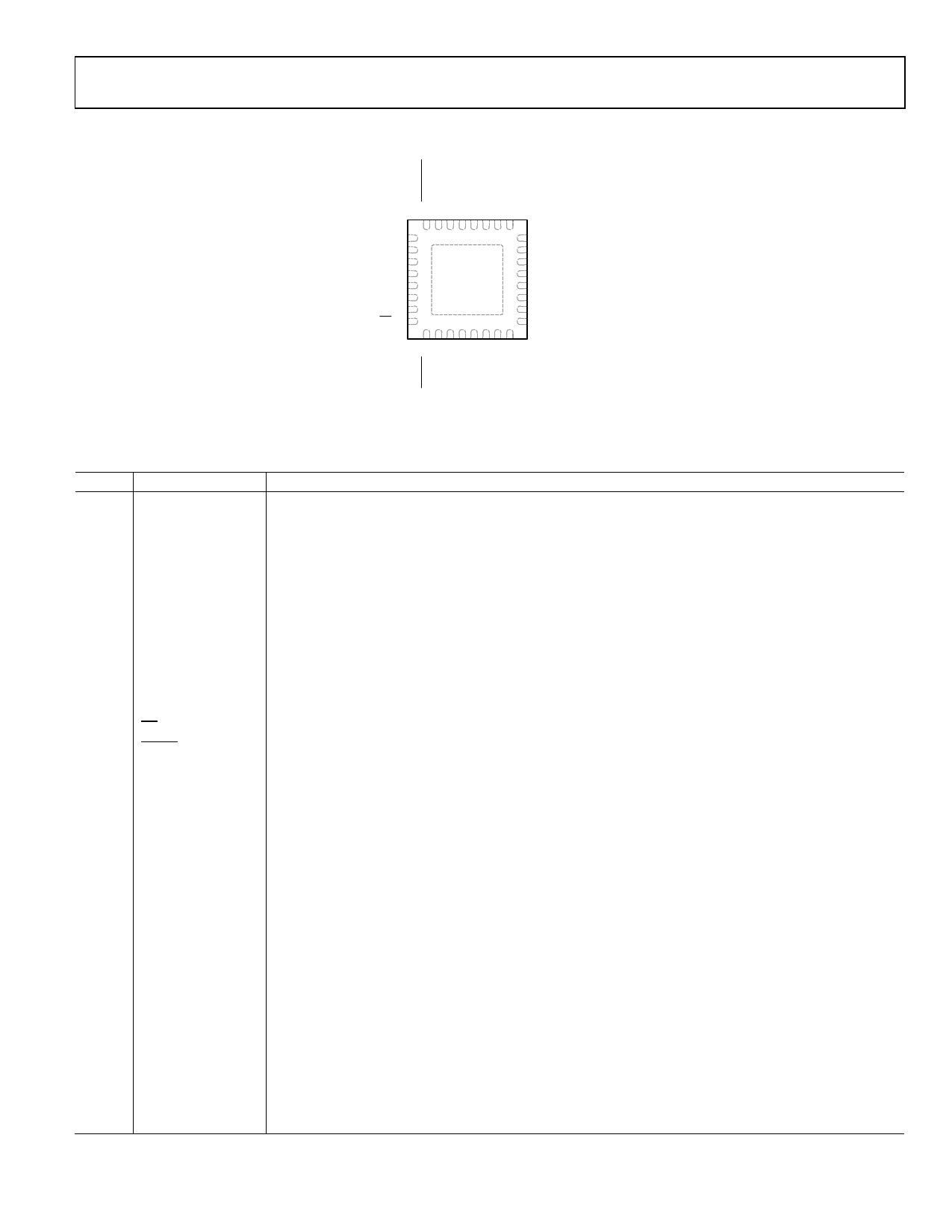
PIN CONFIGURATION AND FUNCTION DESCRIPTIONS
AD9106
SCLK 1
SDIO 2
DGND 3
DLDO2 4
DVDD 5
DLDO1 6
SDO/SDI2/DOUT 7
CS 8
AD9106
TOP VIEW
(Not to Scale)
24 FSADJ2/CAL_SENSE
23 CLKVDD
22 CLDO
21 CLKP
20 CLKN
19 CLKGND
18 REFIO
17 FSADJ4
NOTES
1. THE EXPOSED PAD MUST BE CONNECTED TO DGND.
Figure 2. Pin Configuration
Table 11. Pin Function Descriptions
Pin No. Mnemonic
Description
1 SCLK
SPI Clock Input.
2 SDIO
SPI Data Input/Output. Primary bidirectional data line for the SPI port.
3 DGND
Digital Ground.
4 DLDO2
1.8 V Internal Digital LDO1 Output. When the internal digital LDO1 is enabled, this pin should be bypassed
with a 0.1 µF capacitor.
5 DVDD
3.3 V External Digital Power Supply. DVDD defines the level of the digital interface of the AD9106 (SPI
interface).
6 DLDO1
1.8 V Internal Digital LDO2 Outputs. When the internal digital LDO2 is enabled, this pin should be bypassed
with a 0.1 µFcapacitor.
7
SDO/SDI2/DOUT
Digital I/O Pin.
In 4-wire SPI mode, this pin outputs the data from the SPI.
In double SPI mode, this pin is a second data input line, SDI2, for the SPI port used to write to the SRAM.
In data output mode, this terminal is a programmable pulse output.
8 CSE
A
SPI Port Chip Select, Active Low.
9 RESETE
A
Active Low Reset Pin. Resets registers to their default values.
10 IOUTP4
DAC4 Current Output, Positive Side.
11 IOUTN4
DAC4 Current Output, Negative Side.
12 AVDD2
1.8 V to 3.3 V Power Supply Input for DAC3 and DAC4.
13 IOUTN3
DAC3 Current Output, Negative Side.
14 IOUTP3
DAC3 Current Output, Positive Side.
15 AGND
Analog Ground.
16 FSADJ3
External Full-Scale Current Output Adjust for DAC3.
17 FSADJ4
External Full-Scale Current Output Adjust for DAC4.
18 REFIO
DAC Voltage Reference Input/Output.
19 CLKGND
Clock Ground.
20 CLKN
Clock Input, Negative Side.
21 CLKP
Clock Input, Positive Side.
22 CLDO
Clock Power Supply Output (Internal Regulator in Use), Clock Power Supply Input (Internal Regulator
Bypassed).
23 CLKVDD
Clock Power Supply Input.
24 FSADJ2/CAL_SENSE External Full-Scale Current Output Adjust for DAC2 or Sense Input for Automatic IOUTFS Calibration.
25 FSADJ1
External Full-Scale Current Output Adjust for DAC1 or Full-Scale Current Output Adjust Reference for
Automatic IOUTFS Calibration.
26 AGND
Analog Ground.
27 IOUTP1
DAC1 Current Output, Positive Side.
Rev. A | Page 11 of 48
Free Datasheet http://www.datasheet4u.com/
11 Page | ||
| Páginas | Total 48 Páginas | |
| PDF Descargar | [ Datasheet AD9106.PDF ] | |
Hoja de datos destacado
| Número de pieza | Descripción | Fabricantes |
| AD9100 | Ultrahigh Speed Monolithic Track-and-Hold | Analog Devices |
| AD9101 | 125 MSPS Monolithic Sampling Amplifier | Analog Devices |
| AD9102 | Digital to Analog Converter and Waveform Generator | Analog Devices |
| AD9106 | Digital-to-Analog Converter and Waveform Generator | Analog Devices |
| Número de pieza | Descripción | Fabricantes |
| SLA6805M | High Voltage 3 phase Motor Driver IC. |
Sanken |
| SDC1742 | 12- and 14-Bit Hybrid Synchro / Resolver-to-Digital Converters. |
Analog Devices |
|
DataSheet.es es una pagina web que funciona como un repositorio de manuales o hoja de datos de muchos de los productos más populares, |
| DataSheet.es | 2020 | Privacy Policy | Contacto | Buscar |
