|
|
|
PDF AD8244 Data sheet ( Hoja de datos )
| Número de pieza | AD8244 | |
| Descripción | Precision FET Input Quad Buffer | |
| Fabricantes | Analog Devices | |
| Logotipo | ||
Hay una vista previa y un enlace de descarga de AD8244 (archivo pdf) en la parte inferior de esta página. Total 20 Páginas | ||
|
No Preview Available !
Data Sheet
Single-Supply, Low Power,
Precision FET Input Quad Buffer
AD8244
FEATURES
Low power
250 µA maximum supply current per amplifier
FET input
2 pA maximum input bias current at 25°C
Extremely high input impedance
Low noise
13 nV/√Hz voltage noise at 1 kHz
0.4 µV p-p voltage noise (0.1 Hz to 10 Hz)
0.8 fA/√Hz current noise at 1 kHz
High dc precision
3 µV/°C maximum offset drift (B grade)
3 MHz bandwidth
Unique pinout
No leakage from inputs to supply pins
Provides guarding capability
Rail-to-rail output
Single-supply operation
Input range extends to ground
Wide supply range
Single-supply: 3 V to 36 V
Dual-supply: ±1.5 V to ±18 V
Available in a compact 10-lead MSOP
APPLICATIONS
Biopotential electrodes
Medical instrumentation
High impedance sensor conditioning
Filters
Photodiode amplifiers
GENERAL DESCRIPTION
The AD8244 is a precision, low power, FET input, quad unity-gain
buffer that is designed to isolate very large source impedances
from the rest of the signal chain. The 2 pA maximum bias
current, near zero current noise, and 10 TΩ input impedance
introduce almost no error, even with source impedance well
into the megaohms.
Many traditional operational amplifier pinouts have a supply
pin that is next to the noninverting input. A guard trace must be
routed between these pins to avoid leakage currents much larger
than the bias current of a FET input op amp. Guard traces can
be routed between pins for large packages, such as DIP or even
SOIC; however, the board area consumed by these packages is
prohibitive for many modern applications. The AD8244 solves
this problem with a unique pinout that physically separates the
PIN CONFIGURATION
AD8244
IN A 1
OUT A 2
+VS 3
OUT B 4
IN B 5
10 IN D
9 OUT D
8 –VS
7 OUT C
6 IN C
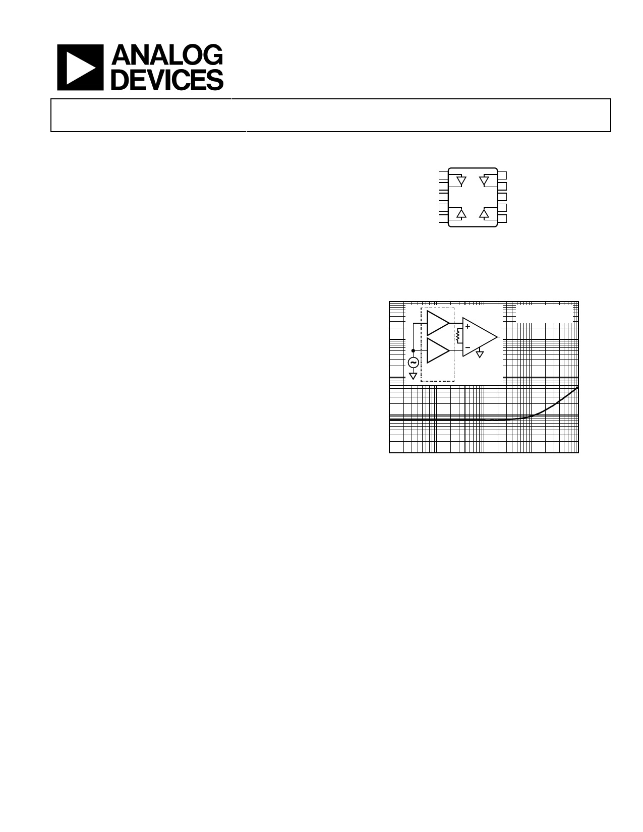
Figure 1.
10
TYPICAL MISMATCH
BETWEEN ANY
TWO CHANNELS
1 IN-AMP
1/2
0.1 AD8244
0.01
0.001
10
100 1k 10k
FREQUENCY (Hz)
Figure 2. Gain Matching vs. Frequency
100k
high impedance inputs from the low impedance supplies and
outputs of the other buffers. This configuration simplifies
guarding while reducing board space, allowing high performance
and high density in the same design.
The AD8244 design is focused on solving problems specific to
buffers. This includes close channel-to-channel matching which
allows channels of the AD8244 to be used in differential signal
chains with minimal error. With its low voltage noise, wide
supply range, and high precision, the AD8244 is also flexible
enough to provide high performance anywhere a unity-gain
buffer is needed, even with low source resistance.
The AD8244 is specified over the industrial temperature range
of −40°C to +85°C. It is available in a 10-lead MSOP package.
Rev. 0
Document Feedback
Information furnished by Analog Devices is believed to be accurate and reliable. However, no
responsibilityisassumedbyAnalogDevices for itsuse,nor foranyinfringementsofpatentsor other
rights of third parties that may result from its use. Specifications subject to change without notice. No
license is granted by implication or otherwise under any patent or patent rights of Analog Devices.
Trademarksandregisteredtrademarksarethepropertyoftheirrespectiveowners.
One Technology Way, P.O. Box 9106, Norwood, MA 02062-9106, U.S.A.
Tel: 781.329.4700
©2013 Analog Devices, Inc. All rights reserved.
Technical Support
www.analog.com
Free Datasheet http://www.datasheet4u.com/
1 page 
Data Sheet
AD8244
VS = ±15 V, TA = 25°C, VIN = 0 V, RL = 10 kΩ, unless otherwise noted.
Table 3.
Parameter
DC PERFORMANCE
Offset Voltage
Over Temperature
Average Temperature Coefficient
Offset Voltage Matching
Input Bias Current
Over Temperature
Input Bias Current Matching
Over Temperature
SYSTEM PERFORMANCE
Nominal Gain
System Error1
Average Temperature Coefficient
Gain Matching
Nonlinearity
NOISE PERFORMANCE
Voltage Noise
Spectral Density
Peak-to-Peak
Current Noise
Spectral Density
Peak-to-Peak
DYNAMIC PERFORMANCE
Small Signal Bandwidth
Slew Rate
Settling Time to 0.01%
INPUT CHARACTERISTICS
Input Voltage Range2
Over Temperature
Input Impedance3
OUTPUT CHARACTERISTICS
Output Swing
Over Temperature
Output Swing
Over Temperature
Short-Circuit Current
Capacitive Load Drive
POWER SUPPLY
Operating Range
Power Supply Rejection
Supply Current per Amplifier
Over Temperature
TEMPERATURE RANGE
Specified Performance
Test Conditions/Comments
TA = −40°C to +85°C
TA = −40°C to +85°C
Channel to channel
TA = 85°C
Channel to channel
TA = 85°C
VOUT = −10 V to +10 V
TA = −40°C to +85°C
Channel to channel
VOUT = −10 V to +10 V
f = 1 kHz
f = 0.1 Hz to 10 Hz
f = 1 kHz
f = 0.1 Hz to 10 Hz
−3 dB
VOUT = −10 V to +10 V
TA = −40°C to +85°C
RL = 10 kΩ
TA = −40°C to +85°C
RL = no load
TA = −40°C to +85°C
Single supply
Dual supply
VS = ±3 V to ±18 V
IOUT = 0 mA
TA = −40°C to +85°C
TA
AD8244A
Min Typ Max
100 600
1.25
10
800
0.9 10
150
0.05
2
1
0.03
2
0.05
5
AD8244B
Min Typ Max
Unit
100 350
0.545
3
500
0.9 3
100
0.05 0.2
2
µV
mV
µV/°C
µV
pA
pA
pA
pA
1 V/V
0.008 %
1 ppm/°C
0.01 %
5 ppm
13 13 nV/√Hz
0.4 0.4 µV p-p
0.8 0.8 fA/√Hz
8 8 fA p-p
3.6 3.6 MHz
0.8 0.8 V/µs
18 18 µs
−15 +14 −15 +14 V
–15 +13.5 –15 +13.5 V
10||4
10||4
TΩ||pF
−14.87
–14.84
−14.95
–14.93
20
200
+14.87
+14.84
+14.95
+14.93
−14.87
–14.84
−14.95
–14.93
20
200
+14.87
+14.84
+14.95
+14.93
V
V
V
V
mA
pF
3 36
±1.5 ±18
90
180 250
300
3 36
±1.5 ±18
80 90
180 250
300
V
V
dB
µA
µA
−40 +85 −40 +85 °C
1 Error as a percentage of the measurement. This includes the effects of open-loop gain and common-mode rejection ratio.
2 The inputs of the AD8244 can go up to the positive supply; however, the input range is derated because error increases near the positive supply as the input
transistors start to saturate.
3 For more information on the input impedance, see Figure 24 and Figure 37.
Rev. 0 | Page 5 of 20
Free Datasheet http://www.datasheet4u.com/
5 Page 
Data Sheet
5
4
3
2
1
–40°C
0 +25°C
+85°C
–1
–2
–3
–4
–5
100 1k 10k 100k
LOAD RESISTANCE (Ω)
Figure 22. Output Voltage Swing vs. Load Resistance
1M
+VS
–0.2
–0.4
–0.6
–0.8
–40°C
+25°C
+85°C
+0.8
+0.6
+0.4
+0.2
–VS
10µ
100µ
1m
OUTPUT CURRENT (A)
Figure 23. Output Voltage Swing vs. Output Current
10m
10
8
6
4
2
VS = ±15V
0 VS = ±5V
–2
–15
–10 –5 0 5 10
INPUT VOLTAGE (V)
Figure 24. Input Bias Current vs. Input Voltage
15
AD8244
25
REPRESENTATIVE SAMPLE
20 VS = ±15V
15
10
5
0
–5
RL = 100kΩ
RL = 10kΩ
–10
–15
–20
–25
–10 –8 –6 –4 –2 0 2 4
OUTPUT VOLTAGE (V)
6
Figure 25. Nonlinearity, VS = ±15 V
8 10
100
REPRESENTATIVE SAMPLE
80 VS = ±5V
60
40
20
0
–20
RL = 100kΩ
RL = 10kΩ
–40
–60
–80
–100
–3
–2 –1 0 1
OUTPUT VOLTAGE (V)
Figure 26. Nonlinearity, VS = ±5 V
2
3
1k
100
10
1
0.1 1 10 100 1k 10k
FREQUENCY (Hz)
Figure 27. Voltage Noise Spectral Density vs. Frequency
Rev. 0 | Page 11 of 20
Free Datasheet http://www.datasheet4u.com/
11 Page | ||
| Páginas | Total 20 Páginas | |
| PDF Descargar | [ Datasheet AD8244.PDF ] | |
Hoja de datos destacado
| Número de pieza | Descripción | Fabricantes |
| AD824 | FET-Input Op Amp | Analog Devices |
| AD8240 | LED Driver/Monitor | Analog Devices |
| AD8244 | Precision FET Input Quad Buffer | Analog Devices |
| Número de pieza | Descripción | Fabricantes |
| SLA6805M | High Voltage 3 phase Motor Driver IC. |
Sanken |
| SDC1742 | 12- and 14-Bit Hybrid Synchro / Resolver-to-Digital Converters. |
Analog Devices |
|
DataSheet.es es una pagina web que funciona como un repositorio de manuales o hoja de datos de muchos de los productos más populares, |
| DataSheet.es | 2020 | Privacy Policy | Contacto | Buscar |