|
|
|
PDF ADP1706 Data sheet ( Hoja de datos )
| Número de pieza | ADP1706 | |
| Descripción | (ADP1706 - ADP1708) CMOS Linear Regulator | |
| Fabricantes | Analog Devices | |
| Logotipo | ||
Hay una vista previa y un enlace de descarga de ADP1706 (archivo pdf) en la parte inferior de esta página. Total 20 Páginas | ||
|
No Preview Available !
FEATURES
Maximum output current: 1 A
Input voltage range: 2.5 V to 5.5 V
Low shutdown current: <1 μA
Low dropout voltage: 345 mV @ 1 A load
Initial accuracy: ±1%
Accuracy over line, load, and temperature: ±2.5%
16 fixed output voltage options with soft start:
0.75 V to 3.3 V (ADP1706)
16 fixed output voltage options with tracking
0.75 V to 3.3 V (ADP1707)
Adjustable output voltage option:
0.8 V to 5.0 V (ADP1708)
Stable with small 4.7 μF ceramic output capacitor
Excellent load/line transient response
Current limit and thermal overload protection
Logic-controlled enable
Available in an 8-lead, exposed paddle SOIC and
3 mm × 3 mm, 8-lead exposed paddle LFCSP
APPLICATIONS
Notebook computers
Memory components
Telecommunications equipment
Network equipment
DSP/FPGA/microprocessor supplies
Instrumentation equipment/data acquisition systems
GENERAL DESCRIPTION
The ADP1706/ADP1707/ADP1708 are CMOS, low dropout
linear regulators that operate from 2.5 V to 5.5 V and provide
up to 1 A of output current. Using an advanced proprietary
architecture, they provide high power supply rejection and
achieve excellent line and load transient response with a small
4.7 μF ceramic output capacitor.
The ADP1706/ADP1707 are available in 16 fixed output volt-
age options. The ADP1708 is available in an adjustable version,
which allows output voltages that range from 0.8 V to 5.0 V via
an external divider. The ADP1706 allows an external soft start
capacitor to be connected to program the start-up time; the
1 A, Low Dropout,
CMOS Linear Regulator
ADP1706/ADP1707/ADP1708
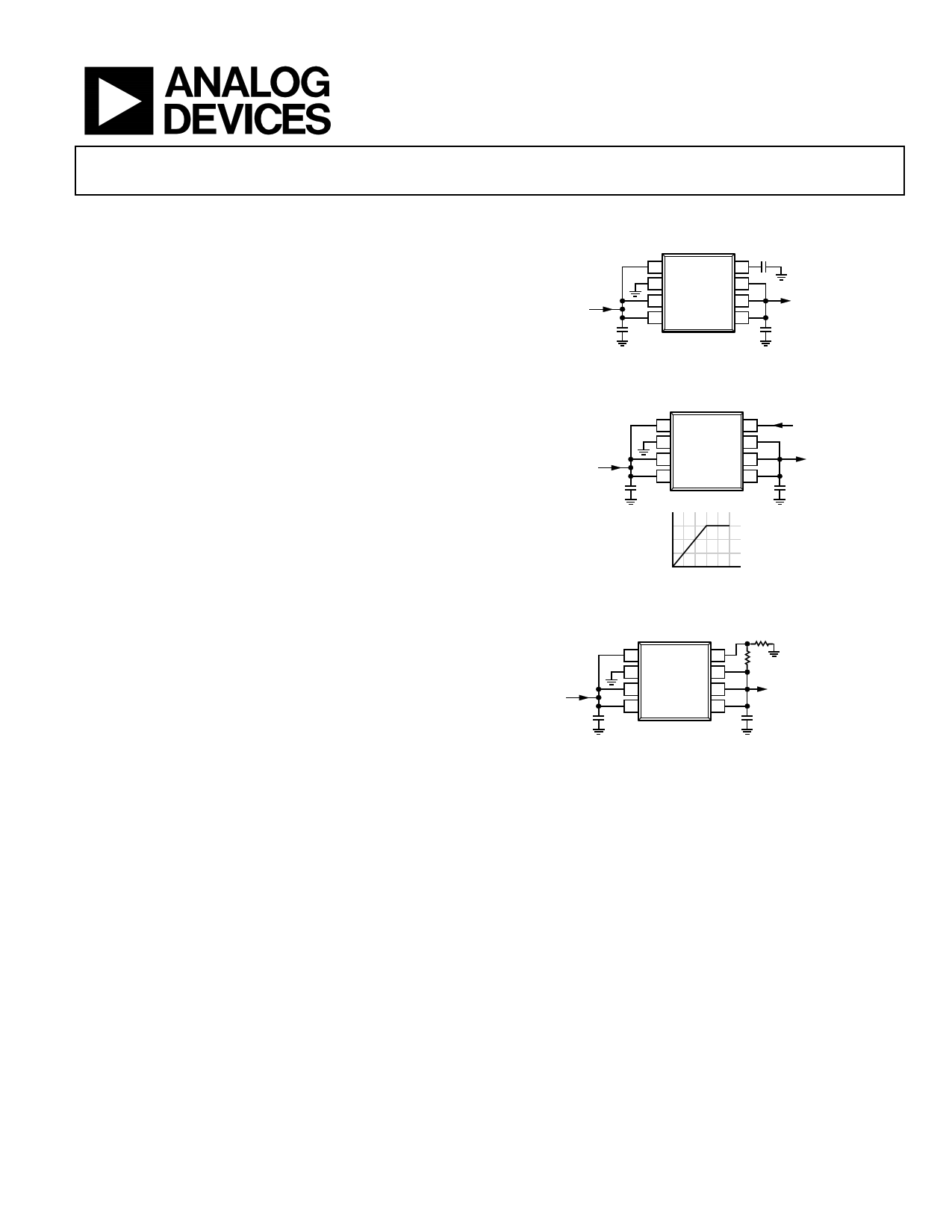
TYPICAL APPLICATION CIRCUITS
VIN = 5V
4.7µF
ADP1706
10nF
1 EN
SS 8
2 GND SENSE 7
3 IN
OUT 6
VOUT = 3.3V
4 IN
OUT 5
4.7µF
Figure 1. ADP1706 with Fixed Output Voltage, 3.3 V
ADP1707
VIN = 5V
4.7µF
1 EN
2 GND
3 IN
4 IN
TRK 8
SENSE 7
OUT 6
OUT 5
VOUT (V)
VTRK
VOUT
4.7µF
3
2
1
0 12345
VTRK (V)
Figure 2. ADP1707 with Output Voltage Tracking
VIN = 5V
4.7µF
ADP1708
1 EN
2 GND
3 IN
4 IN
ADJ 8
SENSE 7
OUT 6
OUT 5
R2
R1
VOUT = 0.8V(1 + R1/R2)
4.7µF
Figure 3. ADP1708 with Adjustable Output Voltage, 0.8 V to 5.0 V
ADP1707 and ADP1708 contain internal soft start capacitors
that give a typical start-up time of 100 μs. The ADP1707
includes a tracking feature that allows the output to follow an
external voltage rail or reference.
The ADP1706/ADP1707/ADP1708 are available in an 8-lead,
exposed paddle SOIC package and an 8-lead, 3 mm × 3 mm
exposed paddle LFCSP, making them not only very compact
solutions but also providing excellent thermal performance for
applications requiring up to 1 A of output current in a small,
low profile footprint.
Rev. 0
Information furnished by Analog Devices is believed to be accurate and reliable. However, no
responsibility is assumed by Analog Devices for its use, nor for any infringements of patents or other
rights of third parties that may result from its use. Specifications subject to change without notice. No
license is granted by implication or otherwise under any patent or patent rights of Analog Devices.
Trademarksandregisteredtrademarksarethepropertyoftheirrespectiveowners.
One Technology Way, P.O. Box 9106, Norwood, MA 02062-9106, U.S.A.
Tel: 781.329.4700
www.analog.com
Fax: 781.461.3113
©2007 Analog Devices, Inc. All rights reserved.
Free Datasheet http://www.datasheet4u.com/
1 page 
ABSOLUTE MAXIMUM RATINGS
Table 2.
Parameter
IN to GND
OUT to GND
EN to GND
SS/ADJ/TRK to GND
SENSE to GND
Storage Temperature Range
Operating Junction Temperature Range
Soldering Conditions
Rating
−0.3 V to +6 V
–0.3 V to IN
–0.3 V to +6 V
–0.3 V to +6 V
–0.3 V to +6 V
–65°C to +150°C
–40°C to +125°C
JEDEC J-STD-020
Stresses above those listed under Absolute Maximum Ratings
may cause permanent damage to the device. This is a stress
rating only; functional operation of the device at these or any
other conditions above those indicated in the operational
section of this specification is not implied. Exposure to absolute
maximum rating conditions for extended periods may affect
device reliability.
ADP1706/ADP1707/ADP1708
THERMAL RESISTANCE
θJA is specified for the worst-case conditions, that is, a device
soldered in a circuit board for surface-mount packages.
Table 3. Thermal Resistance
Package Type
8-Lead SOIC (Exposed Paddle)
8-Lead 3 mm × 3 mm LFCSP (Exposed Paddle)
θJA
58
66
Unit
°C/W
°C/W
ESD CAUTION
Rev. 0 | Page 5 of 20
Free Datasheet http://www.datasheet4u.com/
5 Page 
ADJUSTABLE OUTPUT VOLTAGE (ADP1708)
The ADP1708 can have its output voltage set over a 0.8 V to
5.0 V range. The output voltage is set by connecting a resistive
voltage divider from OUT to ADJ. The output voltage is
calculated by
VOUT = 0.8 V (1 + R1/R2)
(2)
where:
R1 is the resistor from OUT to ADJ.
R2 is the resistor from ADJ to GND.
The maximum bias current into ADJ is 100 nA, so for less
than 0.5% error due to the bias current, use values less than
60 kΩ for R2.
TRACK MODE (ADP1707)
The ADP1707 includes a tracking mode feature. As shown in
Figure 30, if the voltage applied at the TRK pin is less than the
nominal output voltage, OUT is equal to the voltage at TRK.
Otherwise, OUT regulates to its nominal output value.
4.0
3.5
3.0
2.5
2.0
1.5
1.0
0.5
0
0
VIN = 3.8V
VOUT = 3.3V
ILOAD = 10mA
0.5 1.0 1.5 2.0 2.5 3.0 3.5 4.0 4.5 5.0
VTRK (V)
Figure 30. ADP1707 Output Voltage vs. Tracking Voltage
For example, consider an ADP1707 with a nominal output
voltage of 3.3 V. If the voltage applied to its TRK pin is greater
than 3.3 V, OUT maintains a nominal output voltage of 3.3 V.
If the voltage applied to TRK is reduced below 3.3 V, OUT
tracks this voltage. OUT can track the TRK pin voltage from
the nominal value all the way down to 0 V. A voltage divider is
present from TRK to the error amplifier input with a divider
ratio equal to the divider from OUT to the error amplifier,
which sets the output voltage equal to the tracking voltage.
Both divider ratios are set by postpackage trim, depending on
the desired output voltage.
ADP1706/ADP1707/ADP1708
ENABLE FEATURE
The ADP1706/ADP1707/ADP1708 use the EN pin to enable
and disable the OUT pin under normal operating conditions.
As shown in Figure 31, when a rising voltage on EN crosses the
active threshold, OUT turns on. When a falling voltage on EN
crosses the inactive threshold, OUT turns off.
EN
OUT
VIN = 5V
VOUT = 1.6V
COUT = 4.7μF
ILOAD = 10mA
TIME (10ms/DIV)
Figure 31. ADP1706 Typical EN Pin Operation
As shown in Figure 31, the EN pin has hysteresis built in. This
prevents on/off oscillations that can occur due to noise on the
EN pin as it passes through the threshold points.
The EN pin active/inactive thresholds are derived from the IN
voltage. Therefore, these thresholds vary when changing the
input voltage. Figure 32 shows typical EN active/inactive
thresholds when the input voltage varies from 2.5 V to 5.5 V.
1.4
1.3
1.2
1.1 EN ACTIVE
1.0 HYSTERESIS
0.9
0.8
0.7 EN INACTIVE
0.6
0.5
2.50 2.75 3.00 3.25 3.50 3.75 4.00 4.25 4.50 4.75 5.00 5.25 5.50
VIN (V)
Figure 32. Typical EN Pin Thresholds vs. Input Voltage
Rev. 0 | Page 11 of 20
Free Datasheet http://www.datasheet4u.com/
11 Page | ||
| Páginas | Total 20 Páginas | |
| PDF Descargar | [ Datasheet ADP1706.PDF ] | |
Hoja de datos destacado
| Número de pieza | Descripción | Fabricantes |
| ADP170 | (ADP170 / ADP171) CMOS Linear Regulators | Analog Devices |
| ADP1706 | (ADP1706 - ADP1708) CMOS Linear Regulator | Analog Devices |
| ADP1707 | (ADP1706 - ADP1708) CMOS Linear Regulator | Analog Devices |
| ADP1708 | (ADP1706 - ADP1708) CMOS Linear Regulator | Analog Devices |
| Número de pieza | Descripción | Fabricantes |
| SLA6805M | High Voltage 3 phase Motor Driver IC. |
Sanken |
| SDC1742 | 12- and 14-Bit Hybrid Synchro / Resolver-to-Digital Converters. |
Analog Devices |
|
DataSheet.es es una pagina web que funciona como un repositorio de manuales o hoja de datos de muchos de los productos más populares, |
| DataSheet.es | 2020 | Privacy Policy | Contacto | Buscar |