|
|
PDF ADAU1978 Data sheet ( Hoja de datos )
| Número de pieza | ADAU1978 | |
| Descripción | Quad Analog-to-Digital Converter | |
| Fabricantes | Analog Devices | |
| Logotipo |  |
|
Hay una vista previa y un enlace de descarga de ADAU1978 (archivo pdf) en la parte inferior de esta página. Total 44 Páginas | ||
|
No Preview Available !
Data Sheet
Quad Analog-to-Digital Converter (ADC)
ADAU1978
FEATURES
Four 2 V rms differential inputs
On-chip phase-locked loop (PLL) for master clock
Low electromagnetic interference (EMI) design
106 dB analog-to-digital converter (ADC) dynamic range
Total harmonic distortion + noise (THD + N): −95 dB
Selectable digital high-pass filter
24-bit stereo ADC with 8 kHz to 192 kHz sample rates
Digital volume control with autoramp function
I2C/SPI controllable for flexibility
Software-controllable clickless mute
Software power-down
Right justified, left justified, I2S, and TDM modes
Master and slave operation modes
40-lead LFCSP package
Qualified for automotive applications
APPLICATIONS
Automotive audio systems
Active noise cancellation systems
GENERAL DESCRIPTION
The ADAU1978 incorporates four high performance, analog-to-
digital converters (ADCs) with 2 V rms capable ac-coupled inputs.
The ADCs use a multibit sigma-delta (Σ-Δ) architecture with
continuous time front end for low EMI. An I2C/serial peripheral
interface (SPI) control port is included that allows a microcontroller
to adjust volume and many other parameters. The ADAU1978
uses only a single 3.3 V supply. The part internally generates the
required digital DVDD supply. The low power architecture
reduces the power consumption. The ADAU1978 is available in
a 40-lead LFCSP package. The on-chip PLL can derive the master
clock from an external clock input or frame clock (sample rate
clock). When fed with the frame clock, it eliminates the need
for a separate high frequency master clock in the system.
Note that throughout this data sheet, multifunction pins, such
as SCL/CCLK, are referred to either by the entire pin name or
by a single function of the pin, for example, CCLK, when only
that function is relevant.
FUNCTIONAL BLOCK DIAGRAM
AIN1P
AIN1N
AIN2P
AIN2N
AIN3P
AIN3N
AIN4P
AIN4N
ADAU1978
3.3V TO 1.8V
REGULATOR
ADC
ADC
ADC
ADC
AGND1 AGND3
AVDD2
BG
REF
PLL
AGND2
AGND2
I2C/SPI
CONTROL
DVDD
IOVDD
LRCLK
BCLK
SDATAOUT1
SDATAOUT2
SCL/CCLK
SDA/COUT
ADDR1/CIN
ADDR0/CLATCH
PD/RST
Figure 1.
Rev. 0
Document Feedback
Information furnished by Analog Devices is believed to be accurate and reliable. However, no
responsibilityisassumedbyAnalogDevices for itsuse,nor foranyinfringementsofpatentsor other
rights of third parties that may result from its use. Specifications subject to change without notice. No
license is granted by implication or otherwise under any patent or patent rights of Analog Devices.
Trademarksandregisteredtrademarksarethepropertyoftheirrespectiveowners.
One Technology Way, P.O. Box 9106, Norwood, MA 02062-9106, U.S.A.
Tel: 781.329.4700
©2013 Analog Devices, Inc. All rights reserved.
Technical Support
www.analog.com
Free Datasheet http://www.datasheet4u.com/
1 page 
Data Sheet
ADAU1978
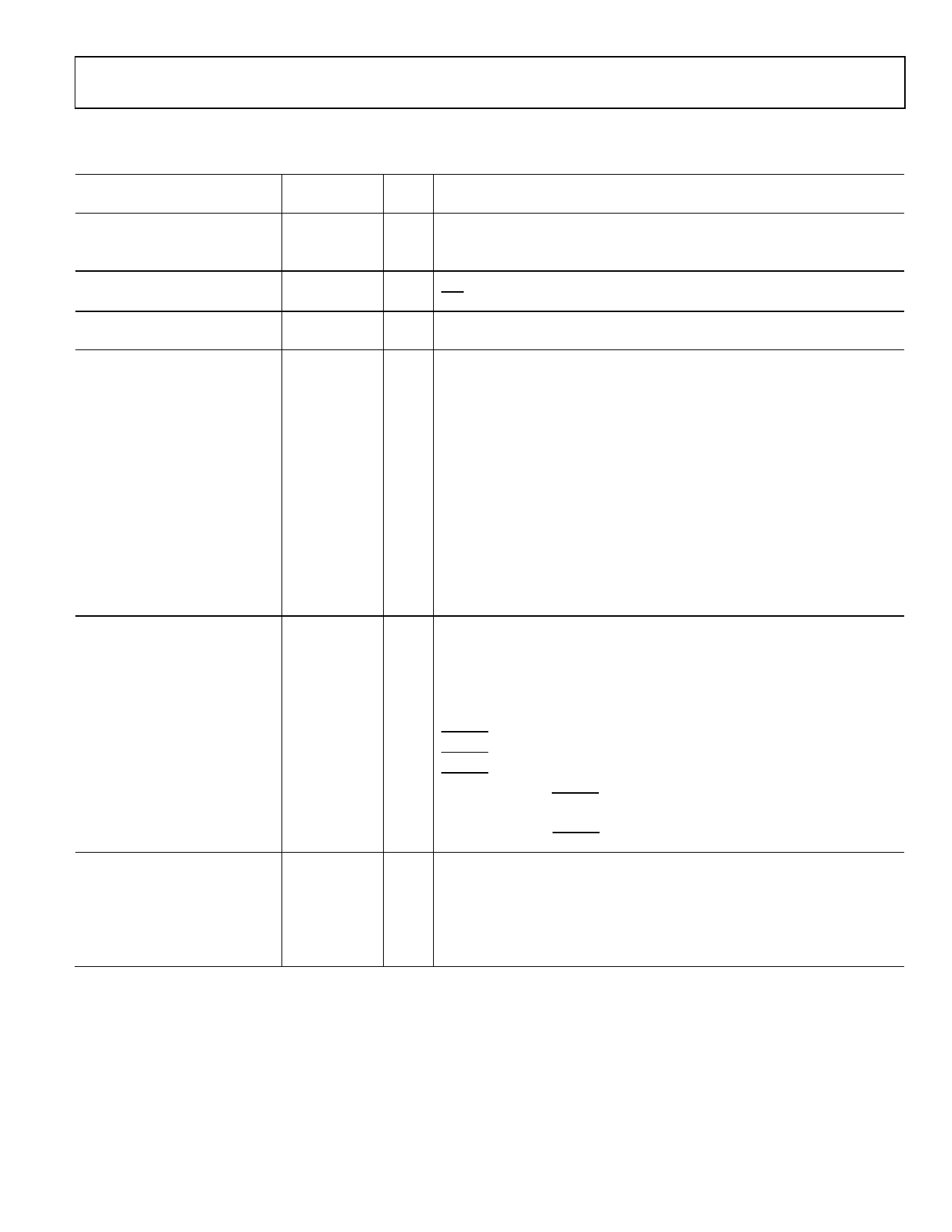
TIMING SPECIFICATIONS
Table 5.
Parameter
INPUT MASTER CLOCK (MCLK)
Duty Cycle
fMCLKIN
RESET
Reset Pulse
PLL
Lock Time
I2C PORT
fSCL
tSCLH
tSCLL
tSCS
tSCH
tDS
tDH
tSCR
tSCF
tSDR
tSDF
tBFT
tSUSTO
SPI PORT
fCCLK
tCCPH
tCCPL
tCDS
tCDH
tCLS
tCLH
tCLPH
tCOE
tCOD
tCOTS
ADC SERIAL PORT
tABH
tABL
tALS
tALH
tABDD
Limit at
Min Max Unit Description
40 60
See Table 9
% MCLKIN duty cycle; MCLKIN at 256 × fS, 384 × fS, 512 × fS, and 768 × fS
MHz MCLKIN frequency, PLL in MCLK mode
15 ns RST low
10
400
0.6
1.3
0.6
0.6
100
0
300
300
300
300
1.3
0.6
10
35
35
10
10
10
40
10
30
30
30
10
10
10
5
18
ms
See Figure 4
kHz SCL frequency
µs SCL high
µs SCL low
µs Setup time; relevant for repeated start condition
µs Hold time; after this period of time, the first clock pulse is generated
ns Data setup time
Data hold time
ns SCL rise time
ns SCL fall time
ns SDA rise time
ns SDA fall time
µs Bus-free time; time between stop and start
µs Setup time for stop condition
see Figure 3
MHz CCLK frequency
ns CCLK high
ns CCLK low
ns CIN setup to CCLK rising
ns CIN hold from CCLK rising
ns CLATCH setup to CCLK rising
ns CLATCH hold from CCLK rising
ns CLATCH high
ns COUT enable from CLATCH falling
ns COUT delay from CCLK falling
ns COUT tristate from CLATCH rising
see Figure 2
ns BCLK high, slave mode
ns BCLK low, slave mode
ns LRCLK setup to BCLK rising, slave mode
ns LRCLK hold from BCLK rising, slave mode
ns SDATAOUTx delay from BCLK falling
Rev. 0 | Page 5 of 44
5 Page 
Data Sheet
0
–10
–20
–30
–40
–50
–60
–70
–80
–90
–100
0 5000 10000 15000 20000 25000 30000 35000 40000
FREQUENCY (Hz)
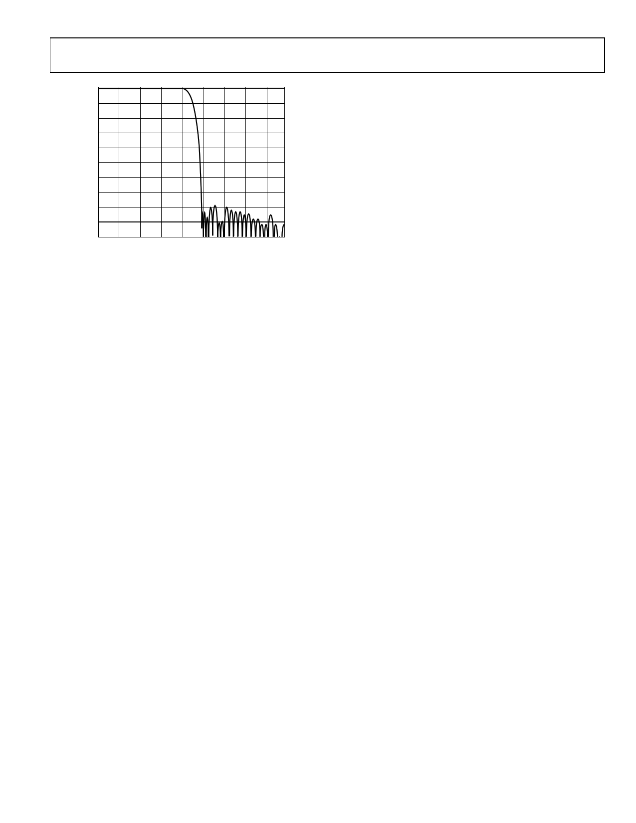
Figure 12. ADC Filter Stop-Band Response at fS = 48 kHz
ADAU1978
Rev. 0 | Page 11 of 44
11 Page | ||
| Páginas | Total 44 Páginas | |
| PDF Descargar | [ Datasheet ADAU1978.PDF ] | |
Hoja de datos destacado
| Número de pieza | Descripción | Fabricantes |
| ADAU1977 | Quad ADC | Analog Devices |
| ADAU1978 | Quad Analog-to-Digital Converter | Analog Devices |
| ADAU1979 | Quad Analog-to-Digital Converter | Analog Devices |
| Número de pieza | Descripción | Fabricantes |
| SLA6805M | High Voltage 3 phase Motor Driver IC. |
Sanken |
| SDC1742 | 12- and 14-Bit Hybrid Synchro / Resolver-to-Digital Converters. |
Analog Devices |
|
DataSheet.es es una pagina web que funciona como un repositorio de manuales o hoja de datos de muchos de los productos más populares, |
| DataSheet.es | 2020 | Privacy Policy | Contacto | Buscar |
