|
|
|
PDF ADP1196 Data sheet ( Hoja de datos )
| Número de pieza | ADP1196 | |
| Descripción | High-Side or Low-Side Load Switch | |
| Fabricantes | Analog Devices | |
| Logotipo | ||
Hay una vista previa y un enlace de descarga de ADP1196 (archivo pdf) en la parte inferior de esta página. Total 12 Páginas | ||
|
No Preview Available !
Data Sheet
5 V, 3 A Logic Controlled
High-Side or Low-Side Load Switch
ADP1196
FEATURES
Low RDSON of 10 mΩ in 6-ball WLCSP
Wide input voltage range: 0 V to 5.5 V
3 A continuous operating current at 70°C
Bias supply voltage range: 1.83 V to 5.5 V
Low 26 µA ground (quiescent) current, VIN ≤ 3.4 V
Low 50 µA quiescent current, VIN = 5.5 V
Overtemperature protection circuitry
Low shutdown current: <3.5 µA
Ultrasmall 1.0 mm × 1.5 mm, 6-ball, 0.5 mm pitch WLCSP
APPLICATIONS
Communications and infrastructure
Thermoelectric cooler (TEC) controller reverse polarity
for heating and cooling
Fine line geometry core voltage inrush current control
Medical and healthcare
Instrumentation
GENERAL DESCRIPTION
The ADP1196 is a high-side or low-side load switch designed for
VIN operation between 0 V and 5.5 V with a VB_EN supply of
1.83 V to 5.5 V. The device contains an internal charge pump that
operates from either VIN or VB_EN, whichever is higher, and
an ultralow on resistance, N-channel MOSFET. This N-channel
MOSFET supports more than 2 A of continuous current at VIN
close to 0 V, and, with its ultralow on resistance, minimizes power
loss. In addition, the on resistance is constant, independent of the
VIN or VB_EN voltage. The low 26 µA quiescent current and
ultralow shutdown current make the ADP1196 ideal for low
power applications.
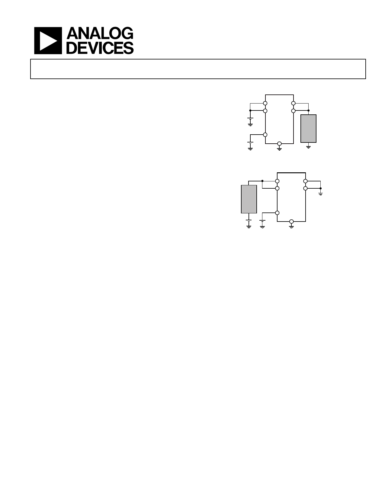
TYPICAL APPLICATIONS CIRCUITS
VIN VOUT
VIN VOUT
+
–
ADP1196
VB_EN
LOAD
+
– GND
Figure 1. Low-Side Load Application
VIN VOUT
VIN VOUT
LOAD
ADP1196
VB_EN
++
––
GND
Figure 2. High-Side Load Application
When the junction temperature exceeds 125°C, overtemperature
http://www.DataSheet4U.com/ protection circuitry is activated, thereby protecting the ADP1196
and downstream circuits from potential damage.
The ADP1196 occupies minimal printed circuit board (PCB)
space, with an area of less than 1.5 mm2 and a height of 0.60 mm.
The ADP1196 is available in an ultrasmall 1.0 mm × 1.5 mm,
6-ball, 0.5 mm pitch WLCSP.
Rev. 0
Document Feedback
Information furnished by Analog Devices is believed to be accurate and reliable. However, no
responsibility is assumed by Analog Devices for its use, nor for any infringements of patents or other
rights of third parties that may result from its use. Specifications subject to change without notice. No
license is granted by implication or otherwise under any patent or patent rights of Analog Devices.
Trademarksandregisteredtrademarksarethepropertyoftheirrespectiveowners.
One Technology Way, P.O. Box 9106, Norwood, MA 02062-9106, U.S.A.
Tel: 781.329.4700
©2013 Analog Devices, Inc. All rights reserved.
Technical Support
www.analog.com
1 page 
Data Sheet
PIN CONFIGURATION AND FUNCTION DESCRIPTIONS
ADP1196
BALL A1
INDICATOR
12
VIN VOUT
A
VIN VOUT
B
VB_EN GND
C
TOP VIEW
(BALL SIDE DOWN)
Not to Scale
Figure 4. Pin Configuration
Table 4. Pin Function Descriptions
Pin No.
Mnemonic Description
A1, B1
VIN Input Voltage.
A2, B2
VOUT
Output Voltage.
C1
VB_EN
Enable/Bias Input. Drive VB_EN high to turn on the switch, and drive VB_EN low to turn off the switch.
C2
GND
Ground.
http://www.DataSheet4U.com/
Rev. 0 | Page 5 of 12
5 Page 
Data Sheet
ADP1196
TIMING
Turn-on delay is defined as the interval between the time that
VVB_EN exceeds the rising threshold voltage and when VOUT rises
to ~10% of its final value. The ADP1196 includes circuitry that has
a typical 2 ms turn-on delay and a controlled rise time to limit
the VIN inrush current. As shown in Figure 25 and Figure 26,
the turn-on delay is nearly independent of the input voltage.
T
2
ENABLE
1
INPUT CURRENT
VOUT
The turn-off time is defined as the time it takes for the output
voltage to fall from 90% to 10% of VOUT. It is also dependent on
the RC time constant of the output capacitance and load resistance.
Figure 27 shows the typical turn-off times with VIN = 1.8 V, VIN =
3.3 V, and VIN = 5.0 V, COUT = 47 μF, and RLOAD = 330 Ω.
6.0 VVB_EN
VIN = 5.0V
5.0
VIN = 3.3V
VIN = 1.8V
4.0
3.0
2.0
1.0
3
CH1 20mAΩ BW
CH3 500mV BW
CH2 1V BW
M1ms
T 10.6%
A CH2 1.18V
Figure 25. Typical Turn-On Time and Inrush Current,
VIN = 1.8 V, COUT = 47 μF, 330 Ω Load
T
2
ENABLE
1
INPUT CURRENT
VOUT
3
CH1 20mAΩ BW
CH3 2V BW
CH2 1V BW
M1ms
T 10.6%
A CH2 1.18V
Figure 26. Typical Turn-On Time and Inrush Current,
VIN = 5 V, COUT = 47 μF, 330 Ω Load
The rise time is defined as the time it takes the output voltage
(VOUT) to rise from 10% to 90% of its final value. The output
voltage rise time is dependent on the rise time of the internal
charge pump.
For very large values of output capacitance, the RC time constant
(where C is the load capacitance (CLOAD) and R is the RDSON||RLOAD)
can become a factor in the rise time of the output voltage. Because
RDSON is much smaller than RLOAD, an adequate approximation
for RC is RDSON × CLOAD. An input or load capacitor is not required
for the ADP1196, although capacitors can be used to suppress
noise on the board.
0
0 0.01 0.02 0.03 0.04 0.05 0.06 0.07 0.08 0.09 0.10
TIME (SEC)
Figure 27. Typical Turn-Off Time, VIN = 1.8 , VIN = 3.3 V, and VIN = 5.0 V,
COUT = 47 μF, RLOAD = 330 Ω
CURRENT-LIMIT AND THERMAL OVERLOAD
PROTECTION
The ADP1196 is protected against damage due to excessive power
dissipation by current and thermal overload protection circuits.
The ADP1196 is designed to limit current when the output load
http://www.DataSheet4U.com/ reaches 4 A. When the output load exceeds 4 A, the output voltage
is reduced to maintain a constant current limit.
Thermal overload protection is included, which limits the junction
temperature to a maximum of 125°C (typical). Under extreme
conditions (that is, high ambient temperature and/or high power
dissipation), when the junction temperature starts to rise above
125°C, the output is turned off, reducing the output current to
zero. When the junction temperature falls below 110°C, the
output is turned on again, and output current is restored to its
operating value.
Consider the case where a hard short from VOUT to GND occurs.
At first, the ADP1196 limits current, so that only 4 A conducts into
the short. If the self-heating of the junction is great enough to
cause its temperature to rise above 125°C, thermal shutdown is
activated, turning off the output and reducing the output current to
zero. As the junction temperature cools and falls below 110°C, the
output turns on and conducts 4 A into the short, again causing the
junction temperature to rise above 125°C. This thermal oscillation
between 110°C and 125°C causes a current oscillation between 4 A
and 0 mA that continues as long as the short remains at the output.
Current and thermal limit protections are intended to protect
the device against accidental overload conditions. For reliable
operation, device power dissipation must be externally limited
so that junction temperature does not exceed 125°C.
Rev. 0 | Page 11 of 12
11 Page | ||
| Páginas | Total 12 Páginas | |
| PDF Descargar | [ Datasheet ADP1196.PDF ] | |
Hoja de datos destacado
| Número de pieza | Descripción | Fabricantes |
| ADP1190 | Integrated 500 mA Load Switch | Analog Devices |
| ADP1190A | Integrated 500 mA Load Switch | Analog Devices |
| ADP1191 | PRECISION SEMICONDUCTOR PRESSURE SENSOR | ETC |
| ADP1196 | High-Side or Low-Side Load Switch | Analog Devices |
| Número de pieza | Descripción | Fabricantes |
| SLA6805M | High Voltage 3 phase Motor Driver IC. |
Sanken |
| SDC1742 | 12- and 14-Bit Hybrid Synchro / Resolver-to-Digital Converters. |
Analog Devices |
|
DataSheet.es es una pagina web que funciona como un repositorio de manuales o hoja de datos de muchos de los productos más populares, |
| DataSheet.es | 2020 | Privacy Policy | Contacto | Buscar |