|
|
|
PDF ADP5052 Data sheet ( Hoja de datos )
| Número de pieza | ADP5052 | |
| Descripción | 5-Channel Integrated Power Solution | |
| Fabricantes | Analog Devices | |
| Logotipo | ||
Hay una vista previa y un enlace de descarga de ADP5052 (archivo pdf) en la parte inferior de esta página. Total 40 Páginas | ||
|
No Preview Available !
Data Sheet
5-Channel Integrated Power Solution with Quad
Buck Regulators and 200 mA LDO Regulator
ADP5052
FEATURES
Wide input voltage range: 4.5 V to 15 V
±1.5% output accuracy over full temperature range
250 kHz to 1.4 MHz adjustable switching frequency
Adjustable/fixed output options via factory fuse
Power regulation
Channel 1 and Channel 2: programmable 1.2 A/2.5 A/4 A
sync buck regulators with low-side FET driver
Channel 3 and Channel 4: 1.2 A sync buck regulators
Channel 5: 200 mA low dropout (LDO) regulator
Always alive 5.1 V LDO supply for tiny load demand
Single 8 A output (Channel 1 and Channel 2 operated
in parallel)
Precision enable with 0.8 V accurate threshold
Active output discharge switch
FPWM or automatic PWM/PSM mode selection
Frequency synchronization input or output
Optional latch-off protection on OVP/OCP failure
Power-good flag on selected channels
UVLO, OCP, and TSD protection
48-lead, 7 mm × 7 mm LFCSP package
−40°C to +125°C junction temperature
APPLICATIONS
Small cell base stations
FPGA and processor applications
Security and surveillance
Medical applications
GENERAL DESCRIPTION
The ADP5052 combines four high performance buck regulators
and one 200 mA low dropout (LDO) regulator in a 48-lead LFCSP
package that meets demanding performance and board space
requirements. The device enables direct connection to high input
voltages up to 15 V with no preregulators.
Channel 1 and Channel 2 integrate high-side power MOSFETs and
low-side MOSFET drivers. External NFETs can be used in low-side
power devices to achieve an efficiency optimized solution and
deliver a programmable output current of 1.2 A, 2.5 A, or 4 A.
Combining Channel 1 and Channel 2 in a parallel configuration
can provide a single output with up to 8 A of current.
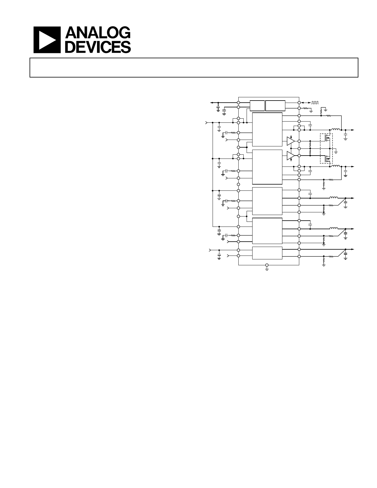
TYPICAL APPLICATION CIRCUIT
C1
4.5V TO 15V
VREG
VDD
C0
PVIN1
C2
COMP1
EN1
SS12
PVIN2
C5
COMP2
EN2
PWRGD
PVIN3
C8
COMP3
EN3
SS34
ADP5052
INT VREG
100mA
OSCILLATOR
CHANNEL 1
BUCK REGULATOR
(1.2A/2.5A/4A)
VREG
CHANNEL 2
BUCK REGULATOR
(1.2A/2.5A/4A)
VREG
SYNC/MODE
RT
FB1
BST1
SW1
C3
DL1 Q1
PGND RILIM1
DL2 RILIM2
SW2
Q2
BST2
FB2
C6
L1 VOUT1
C4
VOUT2
L2
C7
CHANNEL 3
BUCK REGULATOR
(1.2A)
BST3
SW3
C9
FB3
PGND3
BST4
L3 VOUT3
C10
http://www.DataSheet4U.net/
PVIN4
C11
COMP4
EN4
1.7V TO 5.5V PVIN5
C14 EN5
CHANNEL 4
BUCK REGULATOR
(1.2A)
CHANNEL 5
200mA LDO
REGULATOR
C12
SW4
FB4
PGND4
VOUT5
FB5
L4 VOUT4
C13
VOUT5
C15
EXPOSED PAD
Figure 1.
Channel 3 and Channel 4 integrate both high-side and low-side
MOSFETs to deliver output current of 1.2 A.
The switching frequency of the ADP5052 can be programmed
or synchronized to an external clock. The ADP5052 contains a
precision enable pin on each channel for easy power-up sequencing
or adjustable UVLO threshold.
The ADP5052 integrates a general-purpose LDO regulator with
low quiescent current and low dropout voltage that provides up
to 200 mA of output current.
Rev. 0
Document Feedback
Information furnished by Analog Devices is believed to be accurate and reliable. However, no
responsibilityisassumedbyAnalogDevices for itsuse,nor foranyinfringementsofpatentsor other
rights of third parties that may result from its use. Specifications subject to change without notice. No
license is granted by implication or otherwise under any patent or patent rights of Analog Devices.
Trademarksandregisteredtrademarksarethepropertyoftheirrespectiveowners.
One Technology Way, P.O. Box 9106, Norwood, MA 02062-9106, U.S.A.
Tel: 781.329.4700
©2013 Analog Devices, Inc. All rights reserved.
Technical Support
www.analog.com
datasheet pdf - http://www.DataSheet4U.net/
1 page 
Data Sheet
ADP5052
BUCK REGULATOR SPECIFICATIONS
VIN = 12 V, VVREG = 5.1 V, fSW = 600 kHz for all channels, TJ = −40°C to +125°C for minimum and maximum specifications, and TA = 25°C
for typical specifications, unless otherwise noted.
Table 2.
Parameter
CHANNEL 1 SYNC BUCK REGULATOR
FB1 Pin
Fixed Output Options
Adjustable Feedback Voltage
Feedback Voltage Accuracy
Symbol
VOUT1
VFB1
VFB1(DEFAULT)
Feedback Bias Current
SW1 Pin
High-Side Power FET
On Resistance
Current-Limit Threshold
IFB1
RDSON(1H)
ITH(ILIM1)
Minimum On Time
Minimum Off Time
Low-Side Driver, DL1 Pin
Rising Time
Falling Time
Sourcing Resistor
Sinking Resistor
Error Amplifier (EA), COMP1 Pin
EA Transconductance
Soft Start
Soft Start Time
Programmable Soft Start Range
Hiccup Time
COUT Discharge Switch On Resistance
CHANNEL 2 SYNC BUCK REGULATOR
FB2 Pin
Fixed Output Options
Adjustable Feedback Voltage
Feedback Voltage Accuracy
tMIN_ON1
tMIN_OFF1
tRISING1
tFALLING1
tSOURCING1
tSINKING1
gm1
tSS1
tHICCUP1
RDIS1
VOUT2
VFB2
VFB2(DEFAULT)
Feedback Bias Current
SW2 Pin
High-Side Power FET
On Resistance
Current-Limit Threshold
IFB2
RDSON(2H)
ITH(ILIM2)
Minimum On Time
Minimum Off Time
Low-Side Driver, DL2 Pin
Rising Time
Falling Time
Sourcing Resistor
Sinking Resistor
tMIN_ON2
tMIN_OFF2
tRISING2
tFALLING2
tSOURCING2
tSINKING2
Min
0.85
−0.55
−1.25
−1.5
3.50
1.91
4.95
310
2.0
3.3
−0.55
−1.25
−1.5
3.50
1.91
4.95
Typ Max
0.800
1.60
+0.55
+1.0
+1.5
0.1
100
4.4
2.63
6.44
117
1/9 × tSW
5.28
3.08
7.48
155
20
3.4
10
0.95
http://www.DataSheet4U.net/
470
620
2.0
7 × tSS1
250
8.0
0.800
5.0
+0.55
+1.0
+1.5
0.1
110
4.4
2.63
6.44
117
1/9 × tSW
5.28
3.08
7.48
155
20
3.4
10
0.95
Unit Test Conditions/Comments
V Fuse trim
V
% TJ = 25°C
% 0°C ≤ TJ ≤ 85°C
% −40°C ≤ TJ ≤ +125°C
µA Adjustable voltage
mΩ Pin-to-pin measurement
A RILIM1 = floating
A RILIM1 = 47 kΩ
A RILIM1 = 22 kΩ
ns fSW = 250 kHz to 1.4 MHz
ns fSW = 250 kHz to 1.4 MHz
ns CISS = 1.2 nF
ns CISS = 1.2 nF
Ω
Ω
µS
ms SS12 connected to VREG
ms
ms
Ω
V Fuse trim
V
% TJ = 25°C
% 0°C ≤ TJ ≤ 85°C
% −40°C ≤ TJ ≤ +125°C
µA Adjustable voltage
mΩ Pin-to-pin measurement
A RILIM2 = floating
A RILIM2 = 47 kΩ
A RILIM2 = 22 kΩ
ns fSW = 250 kHz to 1.4 MHz
ns fSW = 250 kHz to 1.4 MHz
ns CISS = 1.2 nF
ns CISS = 1.2 nF
Ω
Ω
Rev. 0 | Page 5 of 40
datasheet pdf - http://www.DataSheet4U.net/
5 Page 
Data Sheet
ADP5052
TYPICAL PERFORMANCE CHARACTERISTICS
100
90
80
70
60
50
VOUT = 1.2V
40 VOUT = 1.5V
30
VOUT = 1.8V
VOUT = 2.5V
20
VOUT = 3.3V
VOUT = 5.0V
10
0
01234
IOUT (A)
Figure 4. Channel 1/Channel 2 Efficiency Curve, VIN = 12 V, fSW = 600 kHz,
FPWM Mode
100
90
80
70
60
50
40
VOUT = 1.2V, FPWM
30 VOUT = 1.2V, AUTO PWM/PSM
20
VOUT = 1.8V, FPWM
VOUT = 1.8V, AUTO PWM/PSM
10 VOUT = 3.3V, FPWM
VOUT = 3.3V, AUTO PWM/PSM
0
0 0.1 1 10
IOUT (A)
Figure 7. Channel 1/Channel 2 Efficiency Curve, VIN = 12 V, fSW = 600 kHz,
FPWM and Automatic PWM/PSM Modes
100
90
80
70
60
50
40 VOUT = 1.2V
VOUT = 1.5V
30 VOUT = 1.8V
VOUT = 2.5V
20 VOUT = 3.3V
10
0
01234
IOUT (A)
Figure 5. Channel 1/Channel 2 Efficiency Curve, VIN = 5.0 V, fSW = 600 kHz,
FPWM Mode
http://www.DataSheet4U.net/
100
90
80
70
60
50
VOUT = 1.2V
VOUT = 1.5V
40
VOUT = 1.8V
VOUT = 2.5V
30 VOUT = 3.3V
VOUT = 5.0V
20
10
0
0 0.2 0.4 0.6 0.8 1.0 1.2
IOUT (A)
Figure 8. Channel 3/Channel 4 Efficiency Curve, VIN = 12 V, fSW = 600 kHz,
FPWM Mode
100
90
80
70
fSW = 300kHz
60 fSW = 600kHz
fSW = 1.0MHz
50
40
30
20
10
0
01234
IOUT (A)
Figure 6. Channel 1/Channel 2 Efficiency Curve, VIN = 12 V, VOUT = 1.8 V,
FPWM Mode
100
90
80
70
60
50
VOUT = 1.2V
VOUT = 1.5V
40
VOUT = 1.8V
VOUT = 2.5V
30 VOUT = 3.3V
20
10
0
0 0.2 0.4 0.6 0.8 1.0 1.2
IOUT (A)
Figure 9. Channel 3/Channel 4 Efficiency Curve, VIN = 5.0 V, fSW = 600 kHz,
FPWM Mode
Rev. 0 | Page 11 of 40
datasheet pdf - http://www.DataSheet4U.net/
11 Page | ||
| Páginas | Total 40 Páginas | |
| PDF Descargar | [ Datasheet ADP5052.PDF ] | |
Hoja de datos destacado
| Número de pieza | Descripción | Fabricantes |
| ADP5050 | 5-Channel Integrated Power Solution | Analog Devices |
| ADP5051 | Integrated Power Solution | Analog Devices |
| ADP5052 | 5-Channel Integrated Power Solution | Analog Devices |
| ADP5053 | Integrated Power Solution | Analog Devices |
| Número de pieza | Descripción | Fabricantes |
| SLA6805M | High Voltage 3 phase Motor Driver IC. |
Sanken |
| SDC1742 | 12- and 14-Bit Hybrid Synchro / Resolver-to-Digital Converters. |
Analog Devices |
|
DataSheet.es es una pagina web que funciona como un repositorio de manuales o hoja de datos de muchos de los productos más populares, |
| DataSheet.es | 2020 | Privacy Policy | Contacto | Buscar |