|
|
|
PDF AD9557 Data sheet ( Hoja de datos )
| Número de pieza | AD9557 | |
| Descripción | Dual Input Multiservice Line Card Adaptive Clock Translator | |
| Fabricantes | Analog Devices | |
| Logotipo | ||
Hay una vista previa y un enlace de descarga de AD9557 (archivo pdf) en la parte inferior de esta página. Total 30 Páginas | ||
|
No Preview Available !
Data Sheet
Dual Input Multiservice
Line Card Adaptive Clock Translator
AD9557
FEATURES
Supports GR-1244 Stratum 3 stability in holdover mode
Supports smooth reference switchover with virtually
no disturbance on output phase
Supports Telcordia GR-253 jitter generation, transfer, and
tolerance for SONET/SDH up to OC-192 systems
Supports ITU-T G.8262 synchronous Ethernet slave clocks
Supports ITU-T G.823, G.824, G.825, and G.8261
Auto/manual holdover and reference switchover
2 reference inputs (single-ended or differential)
Input reference frequencies: 2 kHz to 1250 MHz
Reference validation and frequency monitoring (1 ppm)
Programmable input reference switchover priority
20-bit programmable input reference divider
2 pairs of clock output pins, with each pair configurable as
a single differential LVDS/HSTL output or as 2 single-ended
CMOS outputs
Output frequencies: 360 kHz to 1250 MHz
Programmable 17-bit integer and 23-bit fractional
feedback divider in digital PLL
Programmable digital loop filter covering loop bandwidths
from 0.1 Hz to 5 kHz (2 kHz maximum for <0.1 dB of peaking)
Low noise system clock multiplier
Frame sync support
Adaptive clocking
Optional crystal resonator for system clock input
On-chip EEPROM to store multiple power-up profiles
Pin program function for easy frequency translation
configuration
Software controlled power-down
40-lead, 6 mm × 6 mm, LFCSP package
APPLICATIONS
Network synchronization, including synchronous Ethernet
and SDH to OTN mapping/demapping
Cleanup of reference clock jitter
SONET/SDH/OTN clocks up to 100 Gbps, including FEC
Stratum 3 holdover, jitter cleanup, and phase transient control
Wireless base station controllers
Cable infrastructure
Data communications
GENERAL DESCRIPTION
The AD9557 is a low loop bandwidth clock multiplier that
provides jitter cleanup and synchronization for many systems,
including synchronous optical networks (OTN/SONET/SDH).
The AD9557 generates an output clock synchronized to up to
four external input references. The digital PLL allows for
reduction of input time jitter or phase noise associated with
the external references. The digitally controlled loop and
holdover circuitry of the AD9557 continuously generates a low
jitter output clock even when all reference inputs have failed.
The AD9557 operates over an industrial temperature range
of −40°C to +85°C. If more inputs/outputs are needed, refer to
the AD9558 for the four-input/six-output version of the same
device.
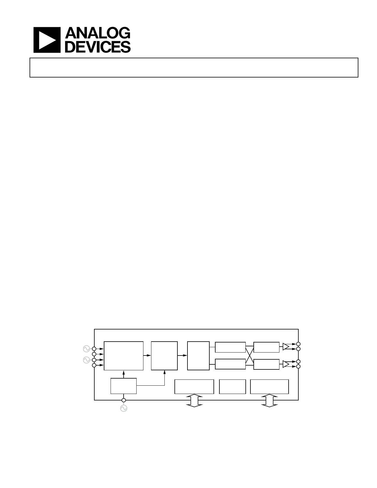
FUNCTIONAL BLOCK DIAGRAM
REFERENCE INPUT
AND
MONITOR MUX
AD9557
DIGITAL
PLL
ANALOG
PLL
÷3 TO ÷11
HF DIVIDER 0
÷3 TO ÷11
HF DIVIDER 1
CHANNEL 0
DIVIDER
CHANNEL 1
DIVIDER
CLOCK
MULTIPLIER
SERIAL INTERFACE
(SPI OR I2C)
EEPROM
STATUS AND
CONTROL PINS
STABLE
SOURCE
Figure 1.
Rev. C
Document Feedback
Information furnished by Analog Devices is believed to be accurate and reliable. However, no
responsibility is assumed by Analog Devices for its use, nor for any infringements of patents or other
rights of third parties that may result from its use. Specifications subject to change without notice. No
license is granted by implication or otherwise under any patent or patent rights of Analog Devices.
Trademarksandregisteredtrademarksarethepropertyoftheirrespectiveowners.
One Technology Way, P.O. Box 9106, Norwood, MA 02062-9106, U.S.A.
Tel: 781.329.4700 ©2011–2016 Analog Devices, Inc. All rights reserved.
Technical Support
www.analog.com
1 page 
AD9557
Changes to Register 0x0405, Table 64.......................................... 73
Changes to Description Column, Register 0x0500, Table 67;
Changes to Description Column, Register 0x0501, Bits[6:4]
and Bit 0, Table 68........................................................................... 74
Change to Description Column, Register 0x0505, Bits[6:4],
Table 70 ............................................................................................ 75
Change to Register 0x0600, Bits[7:2], Table 72 .......................... 76
Changes to Register 0x0707; Change to Register 0x070A,
Bits[3:0], Table 76 ........................................................................... 77
Data Sheet
Changes to Register 0x0A01, Table 87......................................... 79
Changes to Table 96 ....................................................................... 81
Changes to Register 0x0D01, Bit 6 and Bit 1, Table 99.............. 83
Added Table 123 ............................................................................. 89
Changes to Table 124 ..................................................................... 90
Changes to Table 125 ..................................................................... 91
10/2011—Revision 0: Initial Version
Rev. C | Page 4 of 95
5 Page 
AD9557
DISTRIBUTION CLOCK OUTPUTS
Table 10.
Parameter
HSTL MODE
Output Frequency
Rise/Fall Time (20% to 80%)1
Duty Cycle
Up to fOUT = 700 MHz
Up to fOUT = 750 MHz
Up to fOUT = 1250 MHz
Differential Output Voltage Swing
Common-Mode Output Voltage
LVDS MODE
Output Frequency
Rise/Fall Time (20% to 80%)1
Duty Cycle
Up to fOUT = 750 MHz
Up to fOUT = 800 MHz
Up to fOUT = 1250 MHz
Differential Output Voltage Swing
Balanced, VOD
Min
0.36
45
42
700
700
0.36
44
43
247
Typ
140
48
48
43
950
870
185
48
47
43
Unbalanced, ΔVOD
Offset Voltage
Common Mode, VOS
Common-Mode Difference, ΔVOS
Short-Circuit Output Current
CMOS MODE
Output Frequency
1.8 V Supply
3.3 V Supply (OUT0)
Strong Drive Strength Setting
Weak Drive Strength Setting
Rise/Fall Time(20% to 80%)1
1.8 V Supply
3.3 V Supply
Strong Drive Strength Setting
Weak Drive Strength Setting
Duty Cycle
1.8 V Mode
3.3 V Strong Mode
3.3 V Weak Mode
Output Voltage High (VOH)
AVDD3 = 3.3 V, IOH = 10 mA
AVDD3 = 3.3 V, IOH = 1 mA
AVDD3 = 1.8 V, IOH = 1 mA
Output Voltage Low (VOL)
AVDD3 = 3.3 V, IOL = 10 mA
AVDD3 = 3.3 V, IOL = 1 mA
AVDD3 = 1.8 V, IOL = 1 mA
1.125
1.26
13
0.36
0.36
0.36
1.5
0.4
8
50
47
51
AVDD3 − 0.3
AVDD3 − 0.1
AVDD − 0.2
Max
1250
250
52
53
1200
960
1250
280
53
53
454
50
1.375
50
24
150
250
25
3
0.6
0.3
0.1
0.1
Data Sheet
Unit Test Conditions/Comments
MHz
ps 100 Ω termination across output pins
%
%
%
mV Magnitude of voltage across pins; output driver static
mV Output driver static
MHz
ps 100 Ω termination across the output pair
%
%
%
mV Voltage swing between output pins; output driver
static
mV Absolute difference between voltage swing of
normal pin and inverted pin; output driver static
V Output driver static
mV Voltage difference between pins; output driver static
mA Output driver static
MHz 10 pF load
MHz 10 pF load
MHz 10 pF load
ns 10 pF load
ns 10 pF load
ns 10 pF load
% 10 pF load
% 10 pF load
% 10 pF load
Output driver static; strong drive strength
V
V
V
Output driver static; strong drive strength
V
V
V
Rev. C | Page 10 of 95
11 Page | ||
| Páginas | Total 30 Páginas | |
| PDF Descargar | [ Datasheet AD9557.PDF ] | |
Hoja de datos destacado
| Número de pieza | Descripción | Fabricantes |
| AD9550 | Integer-N Clock Translator | Analog Devices |
| AD9551 | Multiservice Clock Generator | Analog Devices |
| AD9552 | Oscillator Frequency Up Converter | Analog Devices |
| AD9553 | Flexible Clock Translator | Analog Devices |
| Número de pieza | Descripción | Fabricantes |
| SLA6805M | High Voltage 3 phase Motor Driver IC. |
Sanken |
| SDC1742 | 12- and 14-Bit Hybrid Synchro / Resolver-to-Digital Converters. |
Analog Devices |
|
DataSheet.es es una pagina web que funciona como un repositorio de manuales o hoja de datos de muchos de los productos más populares, |
| DataSheet.es | 2020 | Privacy Policy | Contacto | Buscar |