|
|
|
PDF ADA4610-2 Data sheet ( Hoja de datos )
| Número de pieza | ADA4610-2 | |
| Descripción | JFET Single/Dual/Quad Op Amps | |
| Fabricantes | Analog Devices | |
| Logotipo | ||
Hay una vista previa y un enlace de descarga de ADA4610-2 (archivo pdf) en la parte inferior de esta página. Total 25 Páginas | ||
|
No Preview Available !
Data Sheet
Low Noise, Precision, Rail-to-Rail Output,
JFET Single/Dual/Quad Op Amps
ADA4610-1/ADA4610-2/ADA4610-4
FEATURES
Low offset voltage
B grade: 0.4 mV maximum (ADA4610-1/ADA4610-2 only)
A grade: 1 mV maximum
Low offset voltage drift
B grade: 4 µV/°C maximum (ADA4610-1/ADA4610-2 only)
A grade: 8 µV/°C maximum (SOIC, MSOP, LFCSP packages)
Low input bias current: 5 pA typical
Dual-supply operation: ±5 V to ±15 V
Low voltage noise: 0.45 µV p-p at 0.1 Hz to 10 Hz
Voltage noise density: 7.30 nV/√Hz at f = 1 kHz
Low total harmonic distortion (THD) + noise: 0.00025%
No phase reversal
Rail-to-rail output
Unity-gain stable
APPLICATIONS
Instrumentation
Medical instruments
Multipole filters
Precision current measurement
Photodiode amplifiers
Sensors
Audio
GENERAL DESCRIPTION
The ADA4610-1/ADA4610-2/ADA4610-4 are precision JFET
amplifiers that feature low input noise voltage, current noise,
offset voltage, input bias current, and rail-to-rail output. The
ADA4610-1 is a single amplifier, the ADA4610-2 is a dual
amplifier, and the ADA4610-4 is a quad amplifier.
The combination of low offset, noise, and very low input bias
current makes these amplifiers especially suitable for high
impedance sensor amplification and precise current measurements
using shunts. With excellent dc precision, low noise, and fast
settling time, the ADA4610-1/ADA4610-2/ADA4610-4 provide
superior accuracy in medical instruments, electronic measurement,
and automated test equipment. Unlike many competitive
amplifiers, the ADA4610-1/ADA4610-2/ADA4610-4 maintain
fast settling performance with substantial capacitive loads. Unlike
many older JFET amplifiers, the ADA4610-1/ADA4610-2/
ADA4610-4 do not suffer from output phase reversal when input
voltages exceed the maximum common-mode voltage range.
The fast slew rate and great stability with capacitive loads make
the ADA4610-1/ADA4610-2/ADA4610-4 perfect fits for high
performance filters. Low input bias currents, low offset, and low
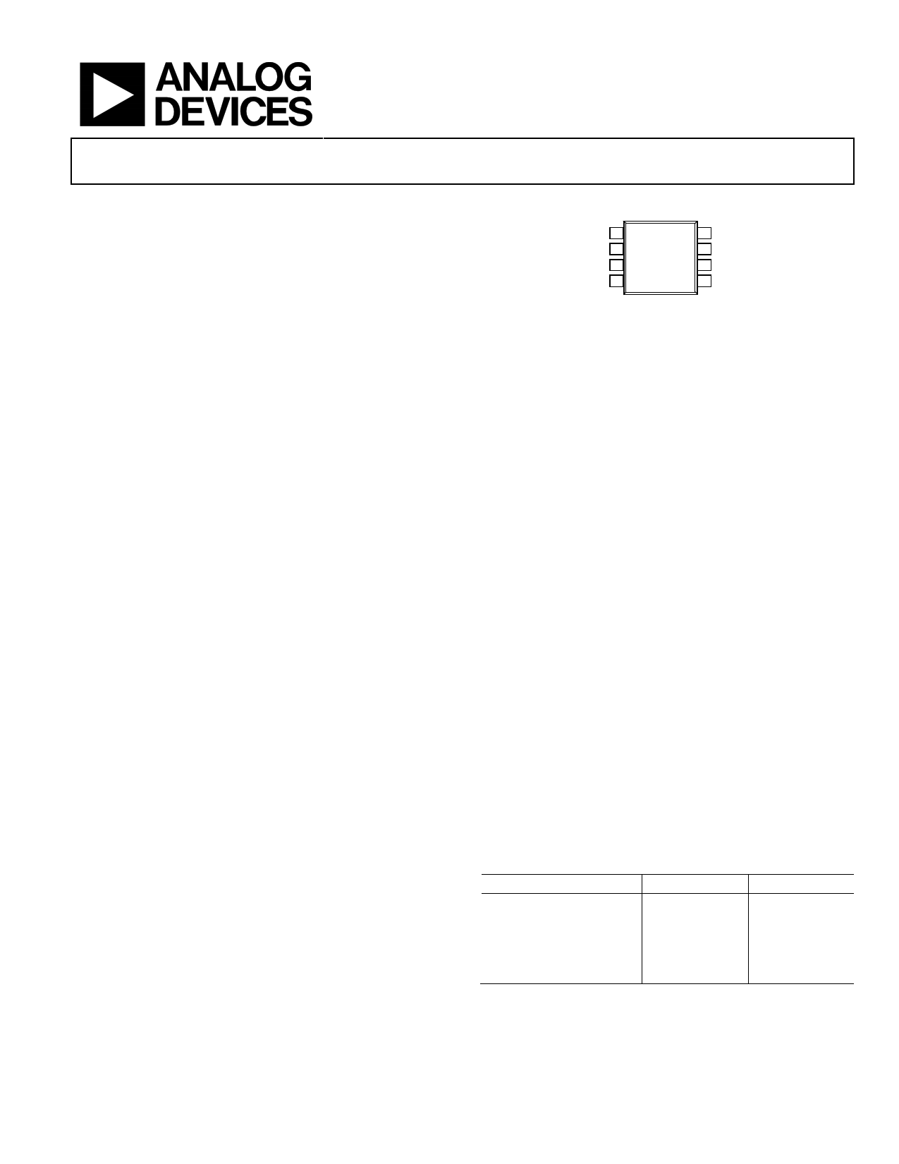
PIN CONFIGURATION
OUT A 1
8 V+
–IN A 2 ADA4610-2 7 OUT B
TOP VIEW
+IN A 3 (Not to Scale) 6 –IN B
V– 4
5 +IN B
Figure 1. ADA4610-2 8-Lead SOIC (R Suffix); for Additional Packages and
Models, See the Pin Configurations and Function Descriptions Section
noise result in a wide dynamic range for photodiode amplifier
circuits. Low noise and distortion, high output current, and
excellent speed make the ADA4610-1/ADA4610-2/ADA4610-4
great choices for audio applications.
The ADA4610-1/ADA4610-2/ADA4610-4 are specified over
the −40°C to +125°C extended industrial temperature range.
The ADA4610-1 is available in an 8-lead SOIC package and in a
5-lead SOT-23 package. The ADA4610-2 is available in 8-lead
SOIC, 8-lead MSOP, and 8-lead LFCSP packages. The ADA4610-4
is available in a 14-lead SOIC package and in a 16-lead LFCSP.
Table 1. Related Precision JFET Operational Amplifiers
Single
Dual
Quad
AD8510
AD8512
AD8513
AD8610
AD8620
Not applicable
AD820
AD822
AD824
ADA4627-1/ADA4637-1 Not applicable Not applicable
Not applicable
ADA4001-2
Not applicable
Rev. G
Document Feedback
Information furnished by Analog Devices is believed to be accurate and reliable. However, no
responsibilityisassumedbyAnalogDevices for itsuse,nor foranyinfringementsofpatentsor other
rights of third parties that may result from its use. Specifications subject to change without notice. No
license is granted by implication or otherwise under any patent or patent rights of Analog Devices.
Trademarksandregisteredtrademarksarethepropertyoftheirrespectiveowners.
One Technology Way, P.O. Box 9106, Norwood, MA 02062-9106, U.S.A.
Tel: 781.329.4700 ©2011–2016 Analog Devices, Inc. All rights reserved.
Technical Support
www.analog.com
1 page 
Data Sheet
ADA4610-1/ADA4610-2/ADA4610-4
Parameter
OUTPUT CHARACTERISTICS
Output Voltage High
Output Voltage Low
Short-Circuit Current
POWER SUPPLY
Power Supply Rejection Ratio
ADA4610-2
ADA4610-1/ADA4610-4
Supply Current per Amplifier
DYNAMIC PERFORMANCE
Slew Rate
Rising
Falling
Gain Bandwidth Product
Unity-Gain Crossover
Phase Margin
−3 dB Closed-Loop Bandwidth
Total Harmonic Distortion (THD) + Noise
NOISE PERFORMANCE
Peak-to-Peak Voltage Noise
Voltage Noise Density
1 Guaranteed by design and characterization.
Symbol Test Conditions/Comments
VOH RL = 2 kΩ
−40°C < TA < +125°C
RL = 600 Ω
−40°C < TA < +125°C
VOL RL = 2 kΩ
−40°C < TA < +125°C
RL = 600 Ω
−40°C < TA < +125°C
ISC
PSRR
VSY = ±4.5 V to ±18 V
−40°C < TA < +125°C
−40°C < TA < +125°C
ISY IOUT = 0 mA
−40°C < TA < +125°C
±SR RL = 2 kΩ, AV = +1
GBP
UGC
φM
−3 dB
THD + N
VIN = 5 mV p-p, RL = 2 kΩ, AV = +100
VIN = 5 mV p-p, RL = 2 kΩ, AV = +1
AV = +1, VIN = 5 mV p-p
1 kHz, AV = +1, RL = 2 kΩ, VIN = 5 V rms
en p-p
en
0.1 Hz to 10 Hz bandwidth
f = 10 Hz
f = 100 Hz
f = 1 kHz
f = 10 kHz
Min Typ
Max Unit
14.80
14.65
14.25
13.35
14.90
14.47
−14.90
−14.68
±79
−14.85
−14.75
−14.60
−14.30
V
V
V
V
V
V
V
V
mA
106 125
103
104 117
100
1.60
dB
dB
dB
dB
1.85 mA
2.0 mA
171 25
171 61
16.3
9.3
66
9.5
0.00025
0.45
14
8.50
7.30
7.30
V/µs
V/µs
MHz
MHz
Degrees
MHz
%
µV p-p
nV/√Hz
nV/√Hz
nV/√Hz
nV/√Hz
Rev. G | Page 5 of 25
5 Page 
Data Sheet
50
40
30
20
10
0
–10
MEAN
–20 MEAN + 3σ
MEAN – 3σ
–30
–40
–50
–5 –4 –3 –2 –1 0 1 2 3 4 5
VCM (V)
Figure 15. Input Bias Current vs. Common-Mode Input Voltage (VCM),
VSY = ±5 V, RL = ∞
100k
10k
SOIC
1k +125°C
100
10
+25°C
1
–40°C
0.1
0.01
–5
–4 –3
–2 –1
012345
VCM (V)
Figure 16. Input Bias Current vs. Common-Mode Input Voltage (VCM),
VSY = ±5 V, RL = ∞
100
10
1
0.1
–50
–25
0 25 50 75
TEMPERATURE (°C)
100 125
Figure 17. Input Bias Current vs. Temperature, VSY = ±5 V
ADA4610-1/ADA4610-2/ADA4610-4
50
40
30
20
10
0
–10 MEAN
MEAN + 3σ
–20 MEAN – 3σ
–30
–40
–50
–15
–10
–5 0 5
VCM (V)
10 15
Figure 18. Input Bias Current vs. Common-Mode Input Voltage (VCM),
VSY = ±15 V, RL = ∞
100k
SOIC
10k
1k
+125°C
100
10
+25°C
1
–40°C
0.1
–15
–10
–5 0
VCM (V)
5
10 15
Figure 19. Input Bias Current vs. Common-Mode Input Voltage (VCM),
VSY = ±15 V, RL = ∞
100
10
1
0.1
–50
–25
0 25 50 75
TEMPERATURE (°C)
100 125
Figure 20. Input Bias Current vs. Temperature, VSY = ±15 V
Rev. G | Page 11 of 25
11 Page | ||
| Páginas | Total 25 Páginas | |
| PDF Descargar | [ Datasheet ADA4610-2.PDF ] | |
Hoja de datos destacado
| Número de pieza | Descripción | Fabricantes |
| ADA4610-1 | JFET Single/Dual/Quad Op Amps | Analog Devices |
| ADA4610-2 | JFET Single/Dual/Quad Op Amps | Analog Devices |
| ADA4610-4 | JFET Dual/Quad Operational Amplifiers | Analog Devices |
| Número de pieza | Descripción | Fabricantes |
| SLA6805M | High Voltage 3 phase Motor Driver IC. |
Sanken |
| SDC1742 | 12- and 14-Bit Hybrid Synchro / Resolver-to-Digital Converters. |
Analog Devices |
|
DataSheet.es es una pagina web que funciona como un repositorio de manuales o hoja de datos de muchos de los productos más populares, |
| DataSheet.es | 2020 | Privacy Policy | Contacto | Buscar |