|
|
|
PDF ADM3251E Data sheet ( Hoja de datos )
| Número de pieza | ADM3251E | |
| Descripción | Single-Channel RS-232 Line Driver/Receiver | |
| Fabricantes | Analog Devices | |
| Logotipo | ||
Hay una vista previa y un enlace de descarga de ADM3251E (archivo pdf) en la parte inferior de esta página. Total 17 Páginas | ||
|
No Preview Available !
Data Sheet
FEATURES
2.5 kV fully isolated (power and data) RS-232 transceiver
isoPower integrated, isolated dc-to-dc converter
460 kbps data rate
1 Tx and 1 Rx
Meets EIA/TIA-232E specifications
ESD protection on RIN and TOUT pins
±8 kV: contact discharge
±15 kV: air gap discharge
0.1 μF charge pump capacitors
High common-mode transient immunity: >25 kV/μs
Safety and regulatory approvals
UL recognition
2500 V rms for 1 minute per UL 1577
VDE Certificate of Conformity
DIN EN 60747-5-2 (VDE 0884 Teil 2): 2003-01
CSA Component Acceptance Notice #5A
Operating temperature range: −40°C to +85°C
Wide body, 20-lead SOIC package
APPLICATIONS
High noise data communications
Industrial communications
General-purpose RS232 data links
Industrial/telecommunications diagnostic ports
Medical equipment
GENERAL DESCRIPTION
The ADM3251E1 is a high speed, 2.5 kV fully isolated, single-
channel RS-232/V.28 transceiver device that operates from a
single 5 V power supply. Due to the high ESD protection on the
RIN and TOUT pins, the device is ideally suited for operation in
electrically harsh environments or where RS-232 cables are
frequently being plugged and unplugged.
The ADM3251E incorporates dual-channel digital isolators
with isoPower™ integrated, isolated power. There is no requirement
to use a separate isolated dc-to-dc converter. Chip-scale trans-
former iCoupler® technology from Analog Devices, Inc., is used
both for the isolation of the logic signals as well as for the inte-
grated dc-to-dc converter. The result is a total isolation solution.
The ADM3251E contains isoPower technology that uses high
frequency switching elements to transfer power through the
Isolated, Single-Channel
RS-232 Line Driver/Receiver
ADM3251E
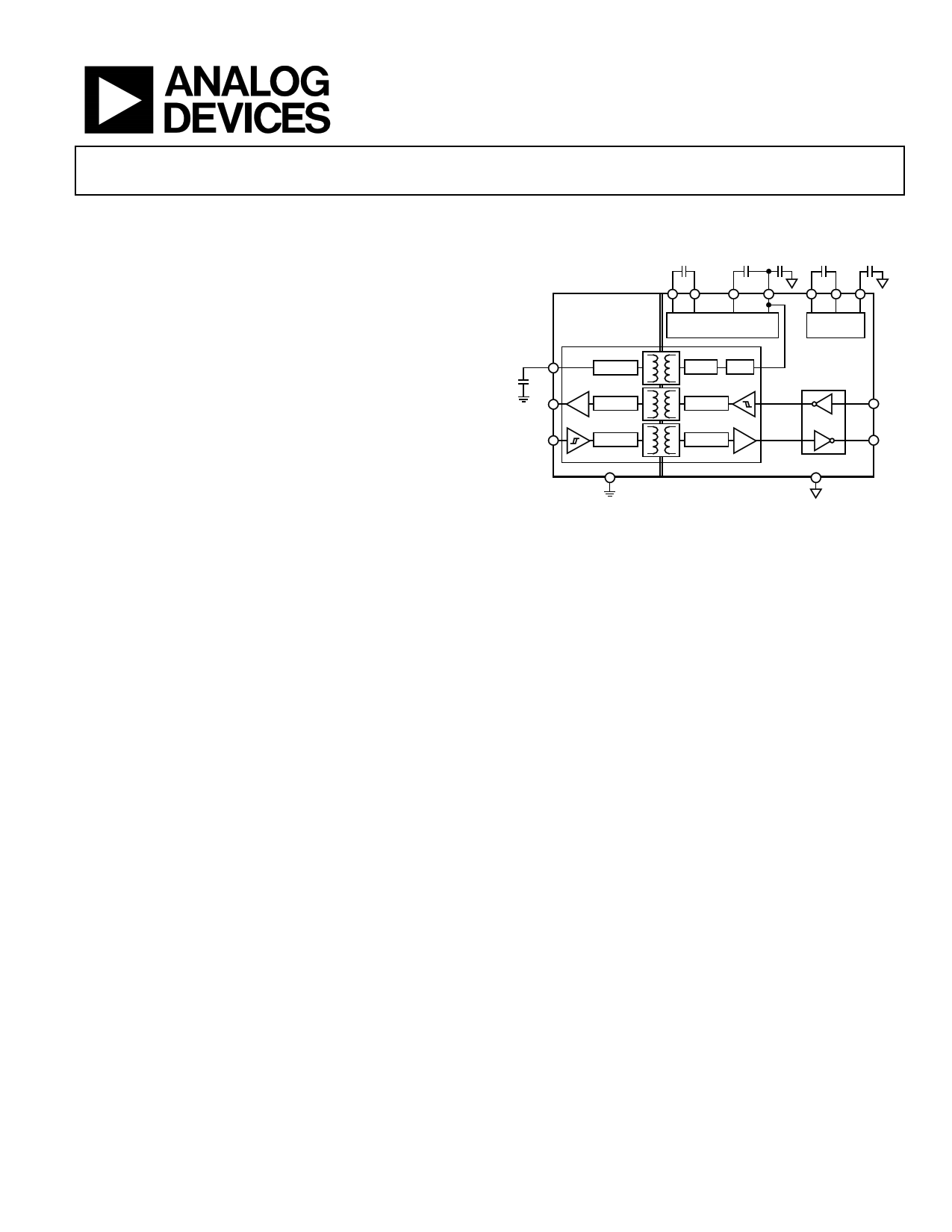
FUNCTIONAL BLOCK DIAGRAM
C1
0.1µF
16V
C3
0.1µF
10V 0.1µF
C2
0.1µF
16V
C4
0.1µF
16V
ADM3251E
VCC
0.1µF
ROUT
TIN
OSC
DECODE
ENCODE
C1+ C1– V+ VISO
VOLTAGE
DOUBLER
C2+ C2– V–
VOLTAGE
INVERTER
RECT REG
ENCODE
DECODE
R RIN*
T TOUT
GND
GNDISO
*INTERNAL 5kΩ PULL-DOWN RESISTOR ON THE RS-232 INPUT.
Figure 1.
transformer. Special care must be taken during printed circuit
board (PCB) layout to meet emissions standards. Refer to
Application Note AN-0971, Control of Radiated Emissions with
isoPower Devices, for details on board layout considerations.
The ADM3251E conforms to the EIA/TIA-232E and ITU-T V. 28
specifications and operates at data rates up to 460 kbps.
Four external 0.1 μF charge pump capacitors are used for the
voltage doubler/inverter, permitting operation from a single
5 V supply.
The ADM3251E is available in a 20-lead, wide body SOIC package
and is specified over the −40°C to +85°C temperature range.
1 Protected by U.S. Patents 5,952,849; 6,873,065; and 7,075,329.
Rev. G
Document Feedback
Information furnished by Analog Devices is believed to be accurate and reliable. However, no
responsibilityisassumedbyAnalogDevices for itsuse,nor foranyinfringementsofpatentsor other
rights of third parties that may result from its use. Specifications subject to change without notice. No
license is granted by implication or otherwise under any patent or patent rights of Analog Devices.
Trademarksandregisteredtrademarksarethepropertyoftheirrespectiveowners.
One Technology Way, P.O. Box 9106, Norwood, MA 02062-9106, U.S.A.
Tel: 781.329.4700 ©2008–2013 Analog Devices, Inc. All rights reserved.
Technical Support
www.analog.com
1 page 
ADM3251E
Data Sheet
All voltages are relative to their respective ground; all minimum/maximum specifications apply over the entire recommended operating
range; TA = 25°C, VCC = 3.3 V (dc-to-dc converter disabled), and the secondary side is powered externally by VISO = 3.3 V, unless
otherwise noted.
Table 2.
Parameter
DC CHARACTERISTICS
VCC Operating Voltage Range
DC-to-DC Converter Disable Threshold, VCC(DISABLE)1
DC-to-DC Converter Disabled
VISO 2
Primary Side Supply Input Current, ICC(DISABLE)
Secondary Side Supply Input Current, IISO(DISABLE)
Secondary Side Supply Input Current, IISO(DISABLE)
LOGIC
Transmitter Input, TIN
Logic Input Current, ITIN
Logic Low Input Threshold, VTINL
Logic High Input Threshold, VTINH
Receiver Output, ROUT
Logic High Output, VROUTH
Logic Low Output, VROUTL
Min
3.0
3.0
−10
0.7 VCC
VCC − 0.1
VCC − 0.5
RS-232
Receiver, RIN
EIA-232 Input Voltage Range3
EIA-232 Input Threshold Low
EIA-232 Input Threshold High
EIA-232 Input Hysteresis
EIA-232 Input Resistance
Transmitter, TOUT
Output Voltage Swing (RS-232)
Transmitter Output Resistance
Output Short-Circuit Current (RS-232)
TIMING CHARACTERISTICS
Maximum Data Rate
Receiver Propagation Delay
tPHL
tPLH
Transmitter Propagation Delay
Transmitter Skew
Receiver Skew
Transition Region Slew Rate3
AC SPECIFICATIONS
Output Rise/Fall Time, tR/tF (10% to 90%)
Common-Mode Transient Immunity at Logic High Output4
Common-Mode Transient Immunity at Logic Low Output4
ESD PROTECTION (RIN AND TOUT PINS)
−30
0.6
3
±5
300
460
5.5
25
25
Typ
6.2
+0.01
VCC
VCC − 0.3
0.0
0.3
1.3
1.6
0.3
5
±5.7
±11
190
135
650
80
55
10
2.3
±15
±8
Max
3.7
3.7
5.5
2.5
12
+10
0.3 VCC
0.1
0.4
+30
2.4
7
30
Unit Test Conditions/Comments
V
V
V
mA No load
mA VISO = 5.5 V, RL = 3 kΩ
mA RL = 3 kΩ
μA
V
V
V IROUTH = −20 μA
V IROUTH = −4 mA
V IROUTH = 20 μA
IROUTH = 4 mA
V
V
V
V
V
kΩ
V RL = 3 kΩ to GND
Ω VISO = 0 V
mA
kbps RL = 3 kΩ to 7 kΩ, CL = 50 pF to 1000 pF
ns
ns
ns RL = 3 kΩ, CL = 1000 pF
ns
ns
V/μs +3 V to −3 V or −3 V to +3 V, VCC = 3.3 V,
RL = 3 kΩ, CL = 1000 pF, TA = 25°C
ns
kV/μs
kV/μs
kV
kV
CL = 15 pF, CMOS signal levels
VCM = 1 kV, transient magnitude = 800 V
VCM = 1 kV, transient magnitude = 800 V
Human body model air discharge
Human body model contact discharge
1 Enable/disable threshold is the VCC voltage at which the internal dc-to-dc converter is enabled/disabled.
2 To maintain data sheet specifications, do not draw current from VISO.
3 Guaranteed by design.
4 VCM is the maximum common-mode voltage slew rate that can be sustained while maintaining specification-compliant operation. VCM is the common-mode potential
difference between the logic and bus sides. The transient magnitude is the range over which the common mode is slewed. The common-mode voltage slew rates
apply to both rising and falling common-mode voltage edges.
Rev. G | Page 4 of 16
5 Page 
ADM3251E
400
350
V–
300
250
200 V+
150
100
50
0
3.00 3.25 3.50 3.75 4.00 4.25 4.50 4.75 5.00 5.25 5.50
VISO (V)
Figure 9. Charge Pump Impedance vs. VISO
200
180
VCC = 5.5V
160
140
120
VCC = 5V
100
VCC = 4.5V
80
60
40
20
0
0 46 92 138 184 230 276 322 368 414 460
DATA RATE (kbps)
Figure 10. Primary Supply Current vs. Data Rate
Data Sheet
1
2
VCC = 5V
LOAD = 3kΩ AND 1nF
TIME (500ns/DIV)
Figure 11. 460 kbps Data Transmission
5.0
4.5
4.0
3.5
3.0
2.5
2.0
1.5
1.0
0.5
0
4.50
HIGH THRESHOLD
LOW THRESHOLD
4.75 5.00 5.25
VCC (V)
Figure 12. TIN Voltage Threshold vs. VCC
5.50
Rev. G | Page 10 of 16
11 Page | ||
| Páginas | Total 17 Páginas | |
| PDF Descargar | [ Datasheet ADM3251E.PDF ] | |
Hoja de datos destacado
| Número de pieza | Descripción | Fabricantes |
| ADM3251E | Single-Channel RS-232 Line Driver/Receiver | Analog Devices |
| Número de pieza | Descripción | Fabricantes |
| SLA6805M | High Voltage 3 phase Motor Driver IC. |
Sanken |
| SDC1742 | 12- and 14-Bit Hybrid Synchro / Resolver-to-Digital Converters. |
Analog Devices |
|
DataSheet.es es una pagina web que funciona como un repositorio de manuales o hoja de datos de muchos de los productos más populares, |
| DataSheet.es | 2020 | Privacy Policy | Contacto | Buscar |