|
|
|
PDF HD74LV1GW57A Data sheet ( Hoja de datos )
| Número de pieza | HD74LV1GW57A | |
| Descripción | Configurable Multiple-Function Gate | |
| Fabricantes | Renesas Technology | |
| Logotipo | ||
Hay una vista previa y un enlace de descarga de HD74LV1GW57A (archivo pdf) en la parte inferior de esta página. Total 9 Páginas | ||
|
No Preview Available !
HD74LV1GW57A
Configurable Multiple–Function Gate
REJ03D0081-0200
Rev.2.00
May 19, 2006
www.DatDaSehesetc4Ur.nipet tion
The HD74LV1GW57A has configurable multiple–function gate in a 6 pin package. The Output state is determined by
eight patterns of 3–bit input. The user can choose the logic functions AND, NAND, NOR, EX–NOR. Low voltage and
high-speed operation is suitable for the battery powered products (e.g., notebook computers), and the low power
consumption extends the battery life.
Features
• The basic gate function is lined up as Renesas uni logic series.
• Supplied on emboss taping for high-speed automatic mounting.
• Supply voltage range : 1.65 to 5.5 V
Operating temperature range : –40 to +85°C
• All inputs VIH (Max.) = 5.5 V (@VCC = 0 V to 5.5 V)
All outputs VO (Max.) = 5.5 V (@VCC = 0 V)
• Output current ±6 mA (@VCC = 3.0 V to 3.6 V), ±12 mA (@VCC = 4.5 V to 5.5 V)
• All the logical input has hysteresis voltage for the slow transition.
• Ordering Information
Part Name
Package Type
Package Code
(Previous Code)
Package
Abbreviation
HD74LV1GW57ACME CMPAK-6 pin
PTSP0006JA-A
(CMPAK-6V)
CM
Taping Abbreviation
(Quantity)
E (3,000 pcs / Reel)
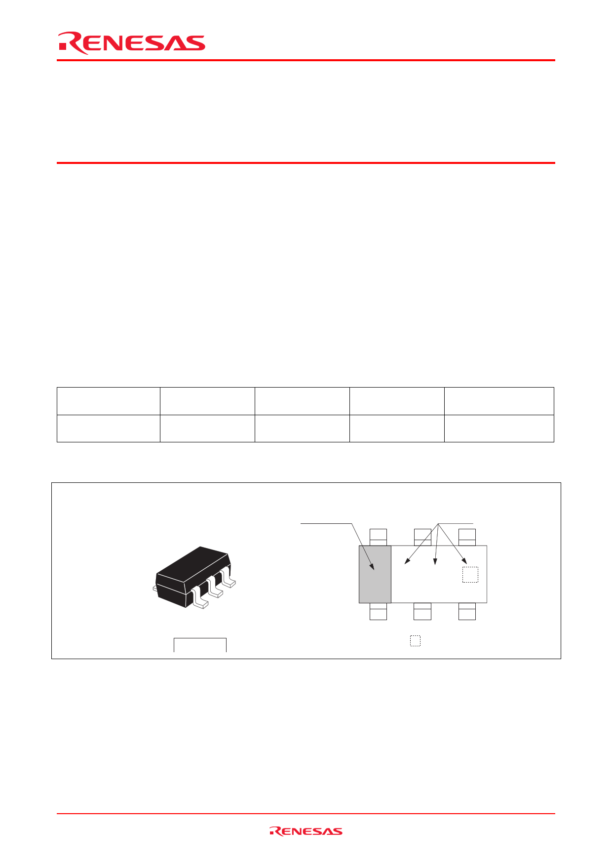
Outline and Article Indication
• HD74LV1GW57A
Index band
Marking
WR
CMPAK–6
= Control code
Rev.2.00, May 19, 2006 page 1 of 8
1 page 
HD74LV1GW57A
Electrical Characteristic
Ta = –40 to 85°C
Item
Symbol VCC (V) *
1.65 to 1.95
VT+
2.5
3.3
Min
—
—
—
Typ Max Unit
— VCC×0.75
— 1.75
— 2.31
Test condition
5.0 — — 3.50
Threshold
voltage
1.65 to 1.95 VCC×0.25
VT–
2.5
3.3
0.75
0.99
—
—
—
—
—
V
—
5.0 1.5 —
—
1.65 to 1.95
2.5
∆VT 3.3
0.1
0.25
0.33
— VCC×0.4
— 1.0
— 1.32
5.0 0.5 — 2.0
Output voltage
Input current
Quiescent
supply current
Output leakage
current
Min to Max VCC–0.1
1.65 1.4
VOH 2.3
2.0
3.0 2.48
4.5 3.8
Min to Max
—
1.65 —
VOL 2.3
—
3.0 —
4.5 —
IIN 0 to 5.5
—
ICC 5.5
—
IOFF
0
—
—
—
—
—
—
—
—
—
—
—
—
—
—
—
—
—
—
—
0.1
0.3
0.4
0.44
0.55
±1
10
5
IOH = –50 µA
IOH = –1 mA
IOH = –2 mA
IOH = –6 mA
V IOH = –12 mA
IOL = 50 µA
IOL = 1 mA
IOL = 2 mA
IOL = 6 mA
IOL = 12 mA
µA VIN = 5.5 V or GND
µA
VIN = VCC or GND,
IO = 0
µA VIN or VO = 0 to 5.5 V
Input capacitance CIN
3.3
—
3.0
— pF VIN = VCC or GND
Note: For conditions shown as Min or Max, use the appropriate values under recommended operating conditions.
Rev.2.00, May 19, 2006 page 5 of 8
5 Page | ||
| Páginas | Total 9 Páginas | |
| PDF Descargar | [ Datasheet HD74LV1GW57A.PDF ] | |
Hoja de datos destacado
| Número de pieza | Descripción | Fabricantes |
| HD74LV1GW57A | Configurable Multiple-Function Gate | Renesas Technology |
| Número de pieza | Descripción | Fabricantes |
| SLA6805M | High Voltage 3 phase Motor Driver IC. |
Sanken |
| SDC1742 | 12- and 14-Bit Hybrid Synchro / Resolver-to-Digital Converters. |
Analog Devices |
|
DataSheet.es es una pagina web que funciona como un repositorio de manuales o hoja de datos de muchos de los productos más populares, |
| DataSheet.es | 2020 | Privacy Policy | Contacto | Buscar |