|
|
|
PDF AD1856 Data sheet ( Hoja de datos )
| Número de pieza | AD1856 | |
| Descripción | 16-Bit PCM Audio DAC | |
| Fabricantes | Analog Devices | |
| Logotipo | ||
Hay una vista previa y un enlace de descarga de AD1856 (archivo pdf) en la parte inferior de esta página. Total 16 Páginas | ||
|
No Preview Available !
Data Sheet
FEATURES
0.0025% THD
Fast settling permits 2×, 4×, and 8× oversampling
±3 V output
Optional trim allows superlinear performance
±5 V to ±12 V operation
16-lead plastic SOIC package
Serial input
APPLICATIONS
Compact disc players
Digital audio amplifiers
DAT recorders and players
Synthesizers and keyboards
GENERAL DESCRIPTION
The AD1856 is a monolithic, 16-bit pulse code modulation (PCM)
audio DAC. The device provides a voltage output amplifier, 16-bit
DAC, 16-bit serial-to-parallel input register, and voltage reference.
The digital portion of the AD1856 is fabricated with CMOS logic
elements that are provided by the Analog Devices, Inc., BiMOS II
process. The analog portion of the AD1856 is fabricated with
bipolar and MOS devices, as well as thin film resistors.
This combination of circuit elements, as well as careful design and
layout techniques, results in high performance audio playback.
Laser trimming of the linearity error affords extremely low total
harmonic distortion. An optional linearity trim pin is provided
to allow residual differential linearity error at midscale to be
eliminated. This feature is particularly valuable for low distortion
reconstructions of low amplitude signals. Output glitch is also
small, contributing to the overall high level of performance. The
output amplifier achieves fast settling and high slew rates, providing
a full ±3 V signal at load currents of up to ±8 mA. The output
amplifier is short-circuit protected and can withstand indefinite
shorts to ground.
The serial input interface consists of the clock, data, and latch
enable pins. The serial twos complement data-word is clocked
into the DAC, MSB first, by the external data clock. The latch
enable signal transfers the input word from the internal serial input
register to the parallel DAC input register. The input clock can
support a 10 MHz clock rate. The serial input port is compatible
with popular digital filter chips used in consumer audio products.
These filters operate at oversampling rates of 2×, 4×, and 8× the
sampling frequency.
16-Bit PCM Audio DAC
AD1856
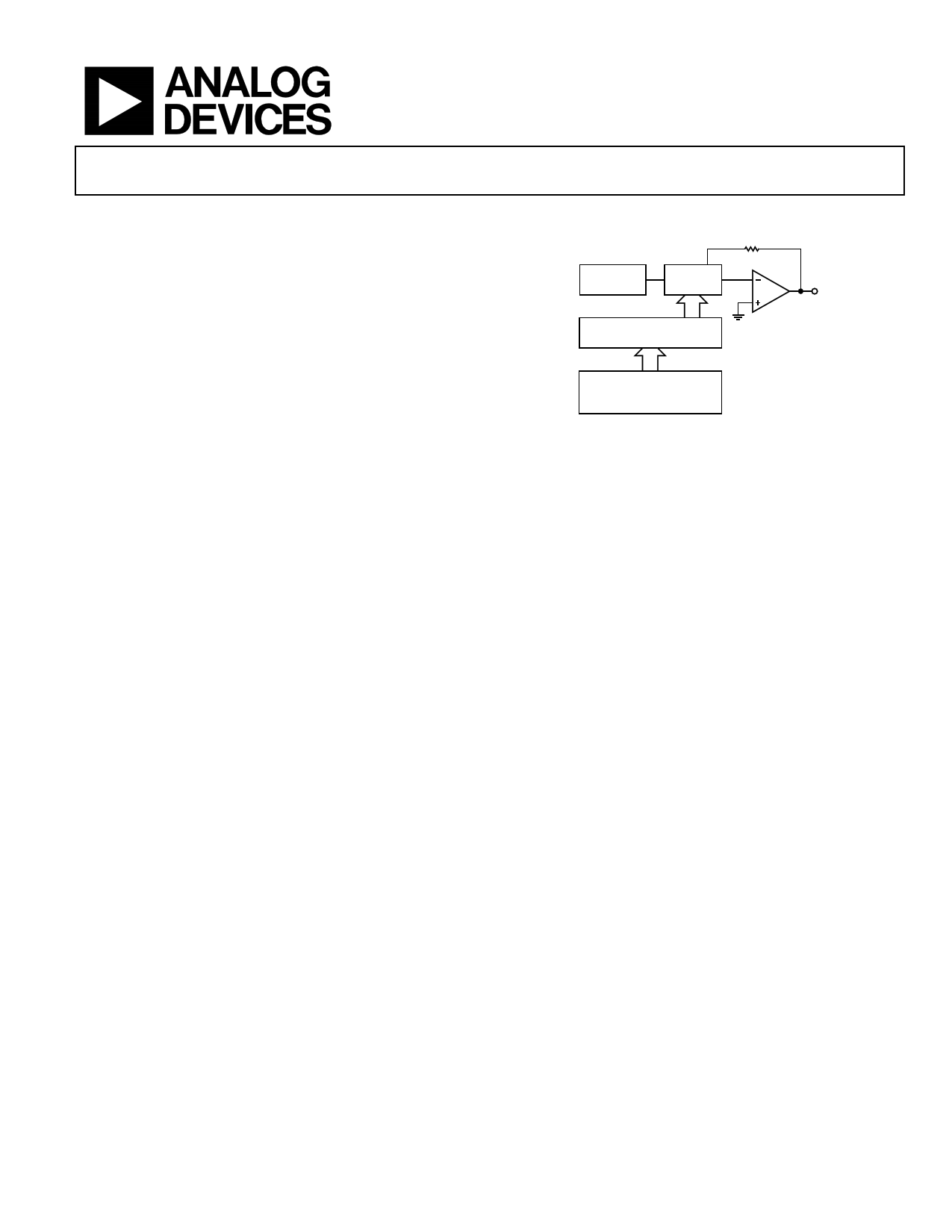
FUNCTIONAL BLOCK DIAGRAM
RF
REFERENCE
16-BIT
IOUT DAC
16-BIT INPUT LATCH
AUDIO
OUTPUT
16-BIT SERIAL-TO-PARALLEL
CONVERSION
CLK
LE DATA
Figure 1.
The AD1856 can operate with ±5 V to ±12 V power supplies,
making it suitable for both the portable and home-use markets.
The digital supplies, +VL and −VL, can be separated from the
analog supplies, +VS and −VS, for reduced digital crosstalk.
Separate analog and digital ground pins are also provided.
Power dissipation is 110 mW (typical) with ±5 V supplies and
135 mW (typical) when ±12 V supplies are used.
The AD1856 is packaged in a 16-lead plastic SOIC package
and incorporates the industry-standard pinout. Operation is
guaranteed over the temperature range of −25°C to +70°C and
over the voltage supply range of ±4.75 V to ±13.2 V.
PRODUCT HIGHLIGHTS
1. Total harmonic distortion is 100% tested.
2. MSB trim feature allows superlinear operation.
3. The AD1856 operates with ±5 V to ±12 V supplies.
4. Serial interface is compatible with digital filter chips.
5. 1.5 μs settling time permits 2×, 4×, and 8× oversampling.
6. No external components are required.
7. 96 dB dynamic range.
8. ±3 V or ±8 mA output capability.
9. 16-bit resolution.
10. Twos complement serial input words.
11. Low cost.
12. 16-lead plastic SOIC package.
Rev. C
Document Feedback
Information furnished by Analog Devices is believed to be accurate and reliable. However, no
responsibility is assumed by Analog Devices for its use, nor for any infringements of patents or other
rights of third parties that may result from its use. Specifications subject to change without notice. No
license is granted by implication or otherwise under any patent or patent rights of Analog Devices.
Trademarksandregisteredtrademarksarethepropertyoftheirrespectiveowners.
One Technology Way, P.O. Box 9106, Norwood, MA 02062-9106, U.S.A.
Tel: 781.329.4700 ©1988–2013 Analog Devices, Inc. All rights reserved.
Technical Support
www.analog.com
1 page 
Data Sheet
ABSOLUTE MAXIMUM RATINGS
Table 2.
Parameter
+VL to DGND
+VS to AGND
−VL to DGND
−VS to AGND
Digital Inputs to DGND
AGND to DGND
Short-Circuit Protection
Soldering, 10 sec
Storage Temperature Range
Rating
0 V to 13.2 V
0 V to 13.2 V
−13.2 V to 0 V
−13.2 V to 0 V
−0.3 V to +VL
±0.3 V
Indefinite short to ground
300°C
−60°C to +100°C
AD1856
Stresses above those listed under Absolute Maximum Ratings
may cause permanent damage to the device. This is a stress
rating only; functional operation of the device at these or any
other conditions above those indicated in the operational
section of this specification is not implied. Exposure to absolute
maximum rating conditions for extended periods may affect
device reliability.
ESD CAUTION
Rev. C | Page 5 of 16
5 Page 
Data Sheet
AD1856
DIGITAL CIRCUIT CONSIDERATIONS
INPUT DATA
Data is transmitted to the AD1856 in a bit stream composed
of 16-bit words with a serial, MSB first format. Three signals
must be present to achieve proper operation: the data, clock,
and latch enable signals. Input data bits are clocked into the
input register on the rising edge of the clock signal. The LSB is
clocked in on the 16th clock pulse. When all data bits are loaded,
a low-going latch enable pulse updates the DAC input. Figure 8
illustrates the general signal requirements for data transfer for
the AD1856.
CLK
Figure 9 provides the specific timing requirements that must be
met for the data transfer to be accomplished properly.
The input pins of the AD1856 are both TTL and 5 V CMOS
compatible, independent of the power supply voltages used.
The input requirements illustrated in Figure 8 and Figure 9
are compatible with the data outputs provided by popular DSP
filter chips used in digital audio playback systems. The AD1856
input clock can run at a 10 MHz rate. This clock rate allows data
transfer rates for 2×, 4×, or 8× oversampling reconstruction. The
Applications of the AD1856 PCM Audio DAC section provides
additional guidelines for using the AD1856 with various DSP
filter chips.
DATA
M
S
B
L
S
B
LE
Figure 8. Signal Requirements of the AD1856
CLK
LATCH
ENABLE (LE)
DATA
>100ns
>30ns >30ns
>60ns >15ns
>40ns >40ns
>50ns
>15ns >15ns
INTERNAL DAC INPUT REGISTER
UPDATED WITH 16 MOST RECENT BITS
MSB
1ST BIT
2ND BIT
LSB
16TH BIT
NEXT
WORD
BITS CLOCKED INTO
SHIFT REGISTER
Figure 9. Timing Relationships of Input Signals
Rev. C | Page 11 of 16
11 Page | ||
| Páginas | Total 16 Páginas | |
| PDF Descargar | [ Datasheet AD1856.PDF ] | |
Hoja de datos destacado
| Número de pieza | Descripción | Fabricantes |
| AD1851 | 16-Bit/18-Bit/ 16 X Fs PCM Audio DACs | Analog Devices |
| AD1852 | Stereo/ 24-Bit/ 192 kHz Multibit DAC | Analog Devices |
| AD1853 | Stereo/ 24-Bit/ 192 kHz/ Multibit DAC | Analog Devices |
| AD1854 | Stereo/ 96 kHz/ Multibit DAC | Analog Devices |
| Número de pieza | Descripción | Fabricantes |
| SLA6805M | High Voltage 3 phase Motor Driver IC. |
Sanken |
| SDC1742 | 12- and 14-Bit Hybrid Synchro / Resolver-to-Digital Converters. |
Analog Devices |
|
DataSheet.es es una pagina web que funciona como un repositorio de manuales o hoja de datos de muchos de los productos más populares, |
| DataSheet.es | 2020 | Privacy Policy | Contacto | Buscar |