|
|
|
PDF PCS3P8504A Data sheet ( Hoja de datos )
| Número de pieza | PCS3P8504A | |
| Descripción | General Purpose Peak EMI Reduction IC | |
| Fabricantes | ON Semiconductor | |
| Logotipo | ||
Hay una vista previa y un enlace de descarga de PCS3P8504A (archivo pdf) en la parte inferior de esta página. Total 6 Páginas | ||
|
No Preview Available !
PCS3P8504A
General Purpose Peak EMI
Reduction IC
Functional Description
PCS3P8504A is a versatile, 3.3 V Timing--Safe Peak EMI
reduction IC. PCS3P8504A accepts an input clock either from a
fundamental Crystal or from an external reference (AC or DC coupled
to XIN/CLKIN) and locks on to it delivering a 1x modulated clock
output. PCS3P8504A has a SSON pin for enabling and disabling
Spread Spectrum function.
PCS3P8504A has an SSEXTR pin to select different deviations
depending upon the value of an external resistor connected between
SSEXTR and GND. Modulation Rate (MR) control selects one of the
two different Modulation Rates.
PCS3P8504A operates from a 3.3 V supply, and is available in an
8--pin, WDFN(2 mm x 2 mm) package.
General Features
1x, LVCMOS Peak EMI Reduction
Input frequency:
15 MHz -- 50 MHz
Output frequency:
15 MHz -- 50 MHz
Analog Deviation Selection
ModRate selection option
Spread Spectrum Enable/Disable
Supply Voltage: 3.3 V ± 0.3 V
8--pin, WDFN 2 mm x 2 mm (TDFN) Package
These Devices are Pb--Free, Halogen Free/BFR Free and are RoHS
Compliant
Application
PCS3P8504A is targeted for consumer electronics application like
DPF, MFP.
www.DataSheet4U.com
http://onsemi.com
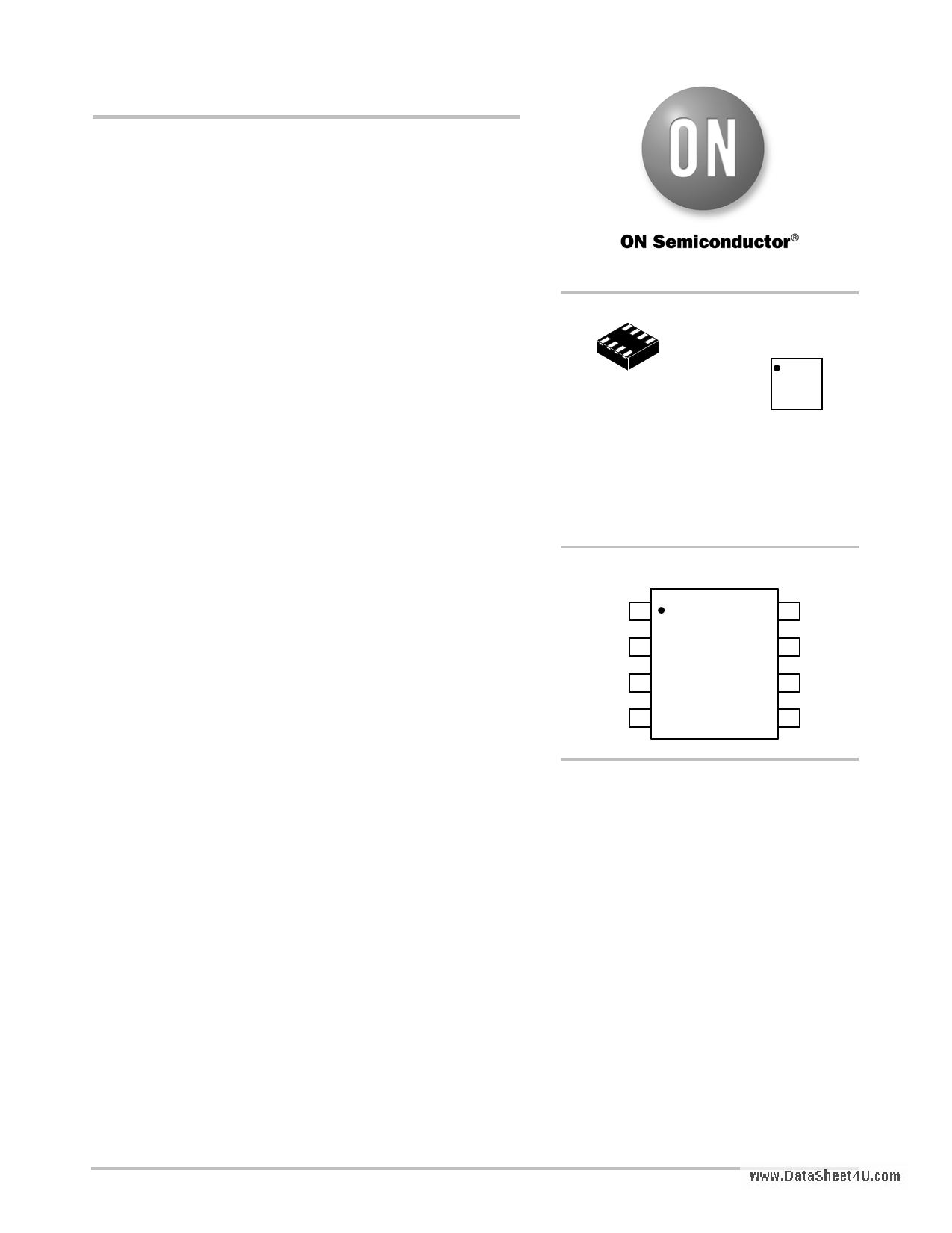
MARKING
DIAGRAMS
1
WDFN8
CASE 511AQ
1 DAMG
G
DA = Specific Device Code
M = Date Code
G = Pb--Free Device
PIN CONFIGURATION
XIN/CLKIN 1
XOUT 2
SSON 3
GND 4
PCS3P8504A
8 VDD
7 SSEXTR
6 MR
5 ModOUT
ORDERING INFORMATION
See detailed ordering and shipping information in the package
dimensions section on page 5 of this data sheet.
Semiconductor Components Industries, LLC, 2010
July, 2010 -- Rev. 1
1
Publication Order Number:
PCS3P8504A/D
1 page 
CL is the load capacitance
for proper XTAL operation
CL
CL VDD
SSON
Control
PCS3P8504A
PCS3P8504A
1 XIN/CLKIN
VDD 8
Noise Reduction Filter
R
C
VDD
2 XOUT
3 SSON
4 GND
SSEXTR 7
MR 6
ModOUT 5
External Deviation Control
www.DataSheet4U.com
VDD
R1
MR Control
Analog Deviation Control
SSEXTR can be Pulled HIGH
to turn OFF Deviation
NOTE: SSON (Pin#3) MR (Pin#6): Connect to VDD or GND
Refer to Pin Description table for Functionality details
Figure 5. Application Schematic
2.5 2.5
MR = 0
MR = 1
2.0 2.0
1.5 1.5
1.0 1.0
0.5 0.5
0.0 0
50 100 150 200 250 300
RESISTANCE (kΩ)
Figure 6. Deviation vs SSEXTR Resistance
Chart at 27 MHz
0.00 50 100 150 200 250 300 350 400 450 500 550 600 650
RESISTANCE (kΩ)
Figure 7. Deviation vs SSEXTR Resistance
Chart at 27 MHz
NOTE: Device to Device variation of Deviation is ±10%
ORDERING INFORMATION
Part Number
Top
Marking
Temperature
Package Type
Shipping†
PCS3P8504AG--08CR
DA
0C to +70C
8--Pin (2 mm x 2 mm) WDFN(TDFN)
Tape & Reel
(Pb--Free)
†For information on tape and reel specifications, including part orientation and tape sizes, please refer to our Tape and Reel Packaging
Specifications Brochure, BRD8011/D.
*A “microdot” placed at the end of last row of marking or just below the last row toward the center of package indicates Pb--Free.
http://onsemi.com
5
5 Page | ||
| Páginas | Total 6 Páginas | |
| PDF Descargar | [ Datasheet PCS3P8504A.PDF ] | |
Hoja de datos destacado
| Número de pieza | Descripción | Fabricantes |
| PCS3P8504A | General Purpose Peak EMI Reduction IC | ON Semiconductor |
| Número de pieza | Descripción | Fabricantes |
| SLA6805M | High Voltage 3 phase Motor Driver IC. |
Sanken |
| SDC1742 | 12- and 14-Bit Hybrid Synchro / Resolver-to-Digital Converters. |
Analog Devices |
|
DataSheet.es es una pagina web que funciona como un repositorio de manuales o hoja de datos de muchos de los productos más populares, |
| DataSheet.es | 2020 | Privacy Policy | Contacto | Buscar |