|
|
PDF ADC1410S Data sheet ( Hoja de datos )
| Número de pieza | ADC1410S | |
| Descripción | Single 14-bit ADC | |
| Fabricantes | NXP Semiconductors | |
| Logotipo | ||
Hay una vista previa y un enlace de descarga de ADC1410S (archivo pdf) en la parte inferior de esta página. Total 30 Páginas | ||
|
No Preview Available !
ADC1410S series
www.DataSheet4U.com
Single 14-bit ADC; 65 Msps, 80 Msps, 105 Msps or 125 Msps;
CMOS or LVDS DDR digital outputs
Rev. 03 — 12 April 2010
Preliminary data sheet
1. General description
The ADC1410S is a single-channel 14-bit Analog-to-Digital Converter (ADC) optimized for
high dynamic performances and low power consumption at sample rates up to 125 Msps.
Pipelined architecture and output error correction ensure the ADC1410S is accurate
enough to guarantee zero missing codes over the entire operating range. Supplied from a
single 3 V source, it can handle output logic levels from 1.8 V to 3.3 V in CMOS mode,
because of a separate digital output supply. It supports the Low Voltage Differential
Signalling (LVDS) Double Data Rate (DDR) output standard. An integrated Serial
Peripheral Interface (SPI) allows the user to easily configure the ADC. The device also
includes a SPI programmable full-scale to allow flexible input voltage range from
1 V to 2 V (peak-to-peak). With excellent dynamic performance from the baseband to
input frequencies of 170 MHz or more, the ADC1410S is ideal for use in communications,
imaging and medical applications.
2. Features and benefits
SNR, 72 dBFS; SFDR, 86 dBc
Sample rate up to 125 Msps
14-bit pipelined ADC core
Clock input divider by 2 for less jitter
contribution
Single 3 V supply
Flexible input voltage range: 1 V to 2 V
(peak-to-peak).
CMOS or LVDS DDR digital outputs
Pin compatible with the ADC1210S
series and the ADC1010S series
HVQFN40 package
Input bandwidth, 600 MHz
Power dissipation, 430 mW at 80 Msps
Serial Peripheral Interface (SPI)
Duty cycle stabilizer
Fast OuT of Range (OTR) detection
INL ±1.5 LSB, DNL ±0.5 LSB
Offset binary, two’s complement, gray
code
Power-down and Sleep modes
3. Applications
Wireless and wired broadband
communications
Spectral analysis
Ultrasound equipment
Portable instrumentation
Imaging systems
Software define radio
1 page 
NXP Semiconductors
ADC1410S series
www.DataSheet4U.com
ADC1410S series; CMOS or LVDS DDR digital output
Table 3. Pin description (LVDS/DDR) digital outputs) …continued
Symbol
Pin [1] Type [2] Description
D0_D1_P 30 O differential output data D0 and D1 multiplexed, true
DAVM
31 O data valid output clock, complement
DAVP
32 O data valid output clock, true
[1] Pins 1 to 16 and pins 33 to 40 are the same for both CMOS and LVDS DDR outputs (see Table 2)
[2] P: power supply; G: ground; I: input; O: output; I/O: input/output.
7. Limiting values
Table 4. Limiting values
In accordance with the Absolute Maximum Rating System (IEC 60134).
Symbol Parameter
Conditions
Min
VO output voltage
pins D13 to D0 or
pins D13P to D0P
and D13M to D0M
−0.4
VDDA
VDDO
Tstg
Tamb
Tj
analog supply voltage
output supply voltage
storage temperature
ambient temperature
junction temperature
−0.4
−0.4
−55
−40
-
Max
+3.9
+3.9
+3.9
+125
+85
125
8. Thermal characteristics
Unit
V
V
V
°C
°C
°C
Table 5.
Symbol
Rth(j-a)
Rth(j-c)
Thermal characteristics
Parameter
thermal resistance from junction to ambient
thermal resistance from junction to case
Conditions
Typ
[1] 22.5
[1] 11.7
[1] Value for six layers board in still air with a minimum of 25 thermal vias.
Unit
K/W
K/W
ADC1410S_SER_3
Preliminary data sheet
All information provided in this document is subject to legal disclaimers.
Rev. 03 — 12 April 2010
© NXP B.V. 2010. All rights reserved.
5 of 37
5 Page 
NXP Semiconductors
ADC1410S series
www.DataSheet4U.com
ADC1410S series; CMOS or LVDS DDR digital output
CLKP
CLKM
DATA
DAV
N N+1
td(s)
tclk
N+2
tPD (N − 14)
(N − 13)
(N − 12)
(N − 11)
tsu th
tPD
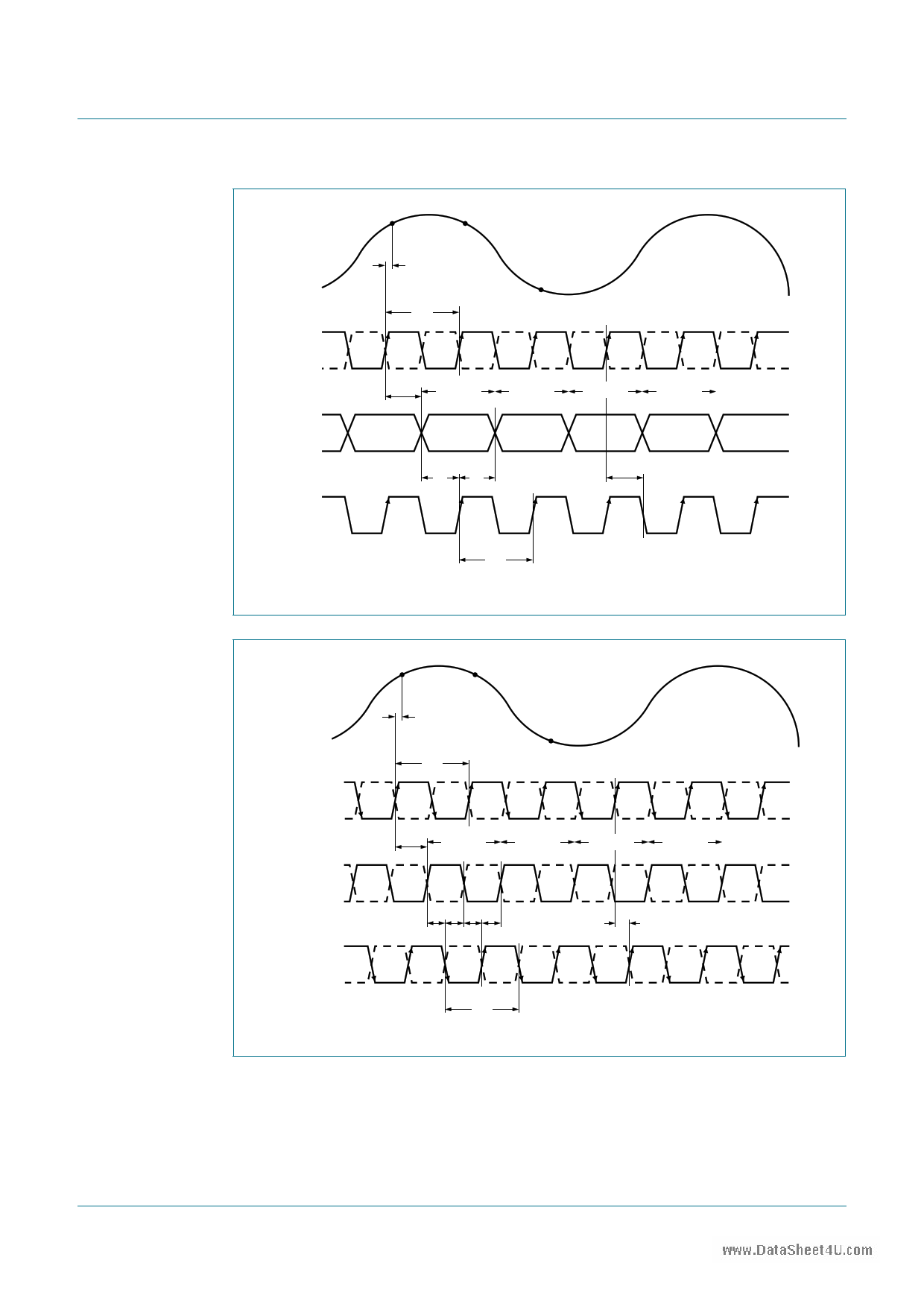
Fig 4. CMOS mode timing
tclk
005aaa060
N N+1
CLKP
td(s)
tclk
N+2
CLKM
Dx_Dx + 1_P
Dx_Dx + 1_M
DAVP
tPD (N − 14)
(N − 13)
(N − 12)
(N − 11)
Dx Dx + 1 Dx Dx + 1 Dx Dx + 1 Dx Dx + 1 Dx Dx + 1
tsu th tsu th
tPD
DAVM
tclk
Fig 5. LDVS DDR mode timing
005aaa061
ADC1410S_SER_3
Preliminary data sheet
All information provided in this document is subject to legal disclaimers.
Rev. 03 — 12 April 2010
© NXP B.V. 2010. All rights reserved.
11 of 37
11 Page | ||
| Páginas | Total 30 Páginas | |
| PDF Descargar | [ Datasheet ADC1410S.PDF ] | |
Hoja de datos destacado
| Número de pieza | Descripción | Fabricantes |
| ADC1410S | Single 14-bit ADC | NXP Semiconductors |
| Número de pieza | Descripción | Fabricantes |
| SLA6805M | High Voltage 3 phase Motor Driver IC. |
Sanken |
| SDC1742 | 12- and 14-Bit Hybrid Synchro / Resolver-to-Digital Converters. |
Analog Devices |
|
DataSheet.es es una pagina web que funciona como un repositorio de manuales o hoja de datos de muchos de los productos más populares, |
| DataSheet.es | 2020 | Privacy Policy | Contacto | Buscar |
