|
|
|
PDF ADC108S052 Data sheet ( Hoja de datos )
| Número de pieza | ADC108S052 | |
| Descripción | 10-Bit A/D Converter | |
| Fabricantes | National Semiconductor | |
| Logotipo | ||
Hay una vista previa y un enlace de descarga de ADC108S052 (archivo pdf) en la parte inferior de esta página. Total 17 Páginas | ||
|
No Preview Available !
September 2005
www.DataSheet4U.com
ADC108S052
8-Channel, 200 kSPS to 500 kSPS, 10-Bit A/D Converter
General Description
The ADC108S052 is a low-power, eight-channel CMOS 10-
bit analog-to-digital converter specified for conversion
throughput rates of 200 kSPS to 500 kSPS. The converter is
based on a successive-approximation register architecture
with an internal track-and-hold circuit. It can be configured to
accept up to eight input signals at inputs IN0 through IN7.
The output serial data is straight binary and is compatible
with several standards, such as SPI™, QSPI™, MICROW-
IRE™, and many common DSP serial interfaces.
The ADC108S052 may be operated with independent ana-
log and digital supplies. The analog supply (VA) can range
from +2.7V to +5.25V, and the digital supply (VD) can range
from +2.7V to VA. Normal power consumption using a +3V or
+5V supply is 1.5 mW and 7.5 mW, respectively. The power-
down feature reduces the power consumption to 0.09 µW
using a +3V supply and 0.30 µW using a +5V supply.
The ADC108S052 is packaged in a 16-lead TSSOP pack-
age. Operation over the extended industrial temperature
range of −40˚C to +105˚C is guaranteed.
Features
n Eight input channels
n Variable power management
n Independent analog and digital supplies
n SPI/QSPI/MICROWIRE/DSP compatible
n Packaged in 16-lead TSSOP
Key Specifications
n Conversion Rate
n DNL (VA = VD = 2.7V to 5.0V)
n INL (VA = VD = 2.7V to 5.0V)
n Power Consumption
— 3V Supply
— 5V Supply
200 kSPS to 500 kSPS
±0.4 LSB (max)
±0.4 LSB (max)
1.5 mW (typ)
7.5 mW (typ)
Applications
n Automotive Navigation
n Portable Systems
n Medical Instruments
n Mobile Communications
n Instrumentation and Control Systems
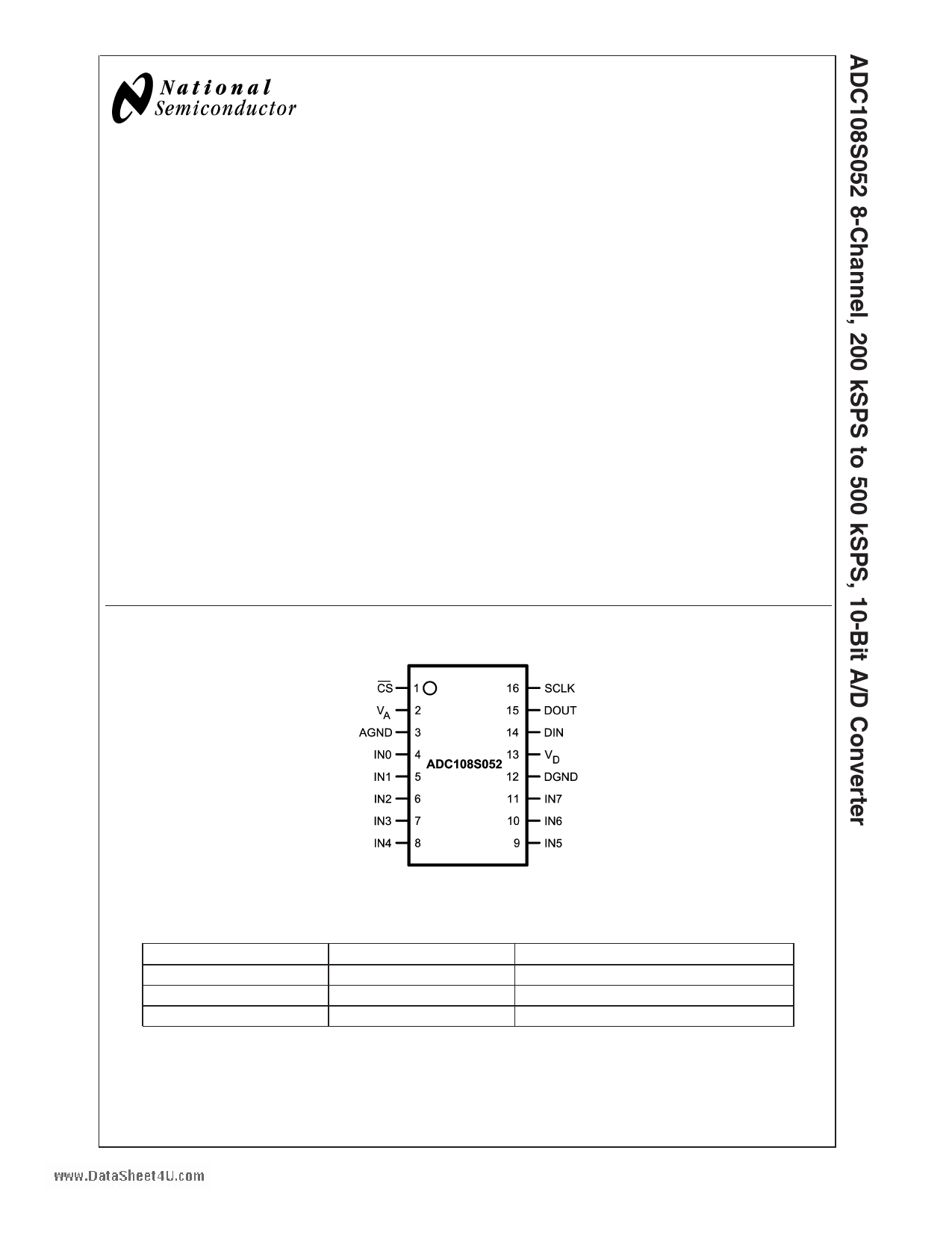
Connection Diagram
Ordering Information
Order Code
ADC108S052CIMT
ADC108S052CIMTX
ADC108S052EVAL
Temperature Range
−40˚C to +105˚C
−40˚C to +105˚C
20164405
Description
16-Lead TSSOP Package
16-Lead TSSOP Package, Tape & Reel
Evaluation Board
TRI-STATE® is a trademark of National Semiconductor Corporation.
MICROWIRE™ is a trademark of National Semiconductor Corporation.
QSPI™ and SPI™ are trademarks of Motorola, Inc.
© 2005 National Semiconductor Corporation DS201644
www.national.com
1 page 
ADC108S052 Timing Specifications
The following specifications apply for VA = VD = +2.7V to +5.25V, AGND = DGND = 0V, fSCLK = 3.2 MHz to 8wMwHwz.,DfaSAtaMSPhLeE e=t4U.com
200 kSPS to 500 kSPS, and CL = 50pF. Boldface limits apply for TA = TMIN to TMAX: all other limits TA = 25˚C.
Symbol
Parameter
Conditions
Typical
Limits
(Note 7)
Units
tCSH
CS Hold Time after SCLK Rising
Edge
(Note 9)
0 10 ns (min)
CS Setup Time prior to SCLK Rising
tCSS
Edge
(Note 9)
5 10 ns (min)
tEN
tDACC
CS Falling Edge to DOUT enabled
DOUT Access Time after SCLK
Falling Edge
5 30 ns (max)
17 27 ns (max)
tDHLD
DOUT Hold Time after SCLK Falling
Edge
4 ns (typ)
DIN Setup Time prior to SCLK
tDS Rising Edge
3 10 ns (min)
DIN Hold Time after SCLK Rising
tDH Edge
3 10 ns (min)
tCH SCLK High Time
tCL SCLK Low Time
CS Rising Edge to DOUT
tDIS High-Impedance
DOUT falling
DOUT rising
0.4 x
tSCLK
ns (min)
0.4 x
tSCLK
ns (min)
2.4 20 ns (max)
0.9 20 ns (max)
Note 1: Absolute Maximum Ratings indicate limits beyond which damage to the device may occur. Operating Ratings indicate conditions for which the device is
functional, but do not guarantee specific performance limits. For guaranteed specifications and test conditions, see the Electrical Characteristics. The guaranteed
specifications apply only for the test conditions listed. Some performance characteristics may degrade when the device is not operated under the listed test
conditions.
Note 2: All voltages are measured with respect to GND = 0V, unless otherwise specified.
Note 3: When the input voltage at any pin exceeds the power supplies (that is, VIN < AGND or VIN > VA or VD), the current at that pin should be limited to 10 mA.
The 20 mA maximum package input current rating limits the number of pins that can safely exceed the power supplies with an input current of 10 mA to two.
Note 4: The absolute maximum junction temperature (TJmax) for this device is 150˚C. The maximum allowable power dissipation is dictated by TJmax, the
junction-to-ambient thermal resistance (θJA), and the ambient temperature (TA), and can be calculated using the formula PDMAX = (TJmax − TA)/θJA. In the 16-pin
TSSOP, θJA is 96˚C/W, so PDMAX = 1,200 mW at 25˚C and 625 mW at the maximum operating ambient temperature of 105˚C. Note that the power consumption
of this device under normal operation is a maximum of 12 mW. The values for maximum power dissipation listed above will be reached only when the ADC108S052
is operated in a severe fault condition (e.g. when input or output pins are driven beyond the power supply voltages, or the power supply polarity is reversed).
Obviously, such conditions should always be avoided.
Note 5: Human body model is 100 pF capacitor discharged through a 1.5 kΩ resistor. Machine model is 220 pF discharged through ZERO ohms
Note 6: Reflow temperature profiles are different for lead-free packages.
Note 7: Tested limits are guaranteed to National’s AOQL (Average Outgoing Quality Level).
Note 8: Data sheet min/max specification limits are guaranteed by design, test, or statistical analysis.
Note 9: Clock may be in any state (high or low) when CS goes high. Setup and hold restrictions apply only to CS going high.
5 www.national.com
5 Page 
Typical Performance Characteristics TA = +25˚C, fSAMPLE = 500 kSPS, fSCLK = 8 MHz, fIN = 40.2
kHz unless otherwise stated. (Continued)
www.DataSheet4U.com
SNR vs. SCLK
THD vs. SCLK
ENOB vs. SCLK
20164462
DNL vs. Temperature
20164465
INL vs. Temperature
20164453
SNR vs. Temperature
20164457
20164460
11
20164463
www.national.com
11 Page | ||
| Páginas | Total 17 Páginas | |
| PDF Descargar | [ Datasheet ADC108S052.PDF ] | |
Hoja de datos destacado
| Número de pieza | Descripción | Fabricantes |
| ADC108S052 | 10-Bit A/D Converter | National Semiconductor |
| ADC108S052 | ADC108S052 8-Channel 200 ksps to 500 ksps 10-Bit A/D Converter (Rev. G) | Texas Instruments |
| Número de pieza | Descripción | Fabricantes |
| SLA6805M | High Voltage 3 phase Motor Driver IC. |
Sanken |
| SDC1742 | 12- and 14-Bit Hybrid Synchro / Resolver-to-Digital Converters. |
Analog Devices |
|
DataSheet.es es una pagina web que funciona como un repositorio de manuales o hoja de datos de muchos de los productos más populares, |
| DataSheet.es | 2020 | Privacy Policy | Contacto | Buscar |