|
|
|
PDF ADS1601 Data sheet ( Hoja de datos )
| Número de pieza | ADS1601 | |
| Descripción | 16-BIT 1.25MSPS ANALOG TO DIGITAL CONVERTER | |
| Fabricantes | Burr-Brown | |
| Logotipo | ||
Hay una vista previa y un enlace de descarga de ADS1601 (archivo pdf) en la parte inferior de esta página. Total 26 Páginas | ||
|
No Preview Available !
ADS1601
www.DataSheet4U.com
16ĆBit, 1.25MSPS
AnalogĆtoĆDigital Converter
SBAS322 − DECEMBER 2004
FEATURES
D High Speed:
Data Rate: 1.25MSPS
Bandwidth: 615kHz
D Outstanding Performance:
SNR: 92dB at fIN = 100kHz, −1dBFS
THD: −103dB at fIN = 100kHz, −6dBFS
SFDR: 105dB at fIN = 100kHz, −6dBFS
D Ease-of-Use:
High-Speed 3-Wire Serial Interface
Directly Connects to TMS320 DSPs
On-Chip Digital Filter Simplifies Anti-Alias
Requirements
Simple Pin-Driven Control—No On-Chip
Registers to Program
Selectable On-Chip Voltage Reference
Simultaneous Sampling with Multiple
ADS1601s
D Low Power:
330mW at 1.25MSPS
145mW at 625kSPS
Power-Down Mode
APPLICATIONS
D Sonar
D Vibration Analysis
D Data Acquisition
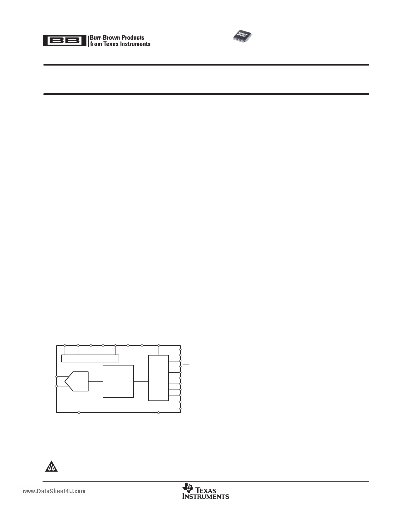
VREFP VREFN VMID RBIAS VCAP AVDD DVDD IOVDD
Reference and Bias Circuits
AINP
AINN
∆Σ
Modulator
Linear Phase
FIR Digital Filter
Serial
Interface
ADS1601
AGND
DGND
CLK
SYNC
FSO
FSO
SCLK
SCLK
DOUT
DOUT
OTR
PD
REFEN
DESCRIPTION
The ADS1601 is a high-speed, high-precision,
delta-sigma analog-to-digital converter (ADC)
manufactured on an advanced CMOS process. The
ADS1601 oversampling topology reduces clock jitter
sensitivity during the sampling of high-frequency, large
amplitude signals by a factor of four over that achieved by
Nyquist-rate ADCs. Consequently, signal-to-noise ratio
(SNR) is particularly improved. Total harmonic distortion
(THD) is −103dB, and the spurious-free dynamic range
(SFDR) is 105dB.
Optimized for power and performance, the ADS1601
dissipates only 330mW while providing a full-scale
differential input range of ±3V. Having such a wide input
range makes out-of-range signals unlikely. The OTR pin
indicates if an analog input out-of-range condition does
occur. The differential input signal is measured against the
differential reference, which can be generated internally or
supplied externally on the ADS1601.
The ADS1601 uses an inherently stable advanced
modulator with an on-chip decimation filter. The filter stop
band extends to 19.3MHz, which greatly simplifies the
anti-aliasing circuitry. The modulator samples the input
signal up to 20MSPS, depending on fCLK, while the 16x
decimation filter uses a series of four half-band FIR filter
stages to provide 75dB of stop band attenuation and
0.001dB of passband ripple.
Output data is provided over a simple 3-wire serial
interface at rates up to 1.25MSPS, with a −3dB bandwidth
of 615kHz. The output data or its complementary format
directly connects to DSPs such as TI’s TMS320 family,
FPGAs, or ASICs. A dedicated synchronization pin
enables simultaneous sampling with multiple ADS1601s
in multi-channel systems. Power dissipation is set by an
external resistor that allows a reduction in dissipation
when operating at slower speeds. All of the ADS1601
features are controlled by dedicated I/O pins, which
simplify operation by eliminating the need for on-chip
registers.
The high performing, easy-to-use ADS1601 is especially
suitable for demanding measurement applications in
sonar, vibration analysis, and data acquisition. The
ADS1601 is offered in a small, 7mm x 7mm TQFP-48
package and is specified from −40°C to +85°C.
Please be aware that an important notice concerning availability, standard warranty, and use in critical applications of Texas Instruments
semiconductor products and disclaimers thereto appears at the end of this data sheet.
All trademarks are the property of their respective owners.
PRODUCTION DATA information is current as of publication date. Products
conform to specifications per the terms of Texas Instruments standard warranty.
Production processing does not necessarily include testing of all parameters.
Copyright 2004, Texas Instruments Incorporated
www.ti.com
1 page 
ADS1601
www.ti.com
wwSwB.ADSa32ta2 S−hDeEeCtE4MUB.cEoRm2004
ELECTRICAL CHARACTERISTICS (continued)
All specifications at TA = −40°C to +85°C, AVDD = 5V, DVDD = IOVDD = 3V, fCLK = 20MHz, VREF = +3V, VCM = +2.7V, and RBIAS = 60kΩ,
unless otherwise noted.
ADS1601
Clock Input
PARAMETER
TEST CONDITIONS
MIN TYP MAX UNIT
Frequency (fCLK)
Duty Cycle
Digital Input/Output
VIH
VIL
VOH
VOL
Input leakage
Power-Supply Requirements
AVDD
DVDD
IOVDD
AVDD current (IAVDD)
DVDD current (IDVDD)
IOVDD current (IIOVDD)
Power dissipation
Temperature Range
Specified
Operating
Storage
fCLK = 20MHz
IOH = 50µA
IOL = 50µA
DGND < VDIGIN < IOVDD
IOH = 50µA
REFEN = low
REFEN = high
IOVDD = 3V
IOVDD = 3V
AVDD = 5V, DVDD = 3V,
IOVDD = 3V, REFEN = high
PD = low, CLK disabled
45
0.7 IOVDD
DGND
IOVDD − 0.5
4.75
2.7
2.7
65
55
15
3
330
10
−40
−40
−60
20
55
IOVDD
0.3 IOVDD
DGND + 0.5
±10
5.25
3.3
5.25
77
65
18
8
380
+85
+105
+150
MHz
%
V
V
V
V
µA
V
V
V
mA
mA
mA
mA
mW
mW
°C
°C
°C
5
5 Page 
ADS1601
www.ti.com
wwSwB.ADSa3t2a2S−hDeEeCtE4MUB.cEoRm2004
TYPICAL CHARACTERISTICS (continued)
All specifications at TA = 25°C, AVDD = 5V, DVDD = IOVDD = 3V, fCLK = 20MHz, VREF = +3V, VCM = +2.7V, and RBIAS = 60kΩ, unless
otherwise noted.
100
95
90
85
80
75
70
10k
SIGNAL−TO−NOISE RATIO
vs INPUT FREQUENCY
VIN = −1dB
VIN = −6dB
VIN = −10dB
100k
Input Frequency, fIN (Hz)
Figure 15
SPURIOUS−FREE DYNAMIC RANGE
vs INPUT FREQUENCY
120
VIN = −10dB
110
VIN = −6dB
100
1M
90
VIN = −1dB
80
10k
100k
Input Frequency, fIN (Hz)
Figure 17
1M
−80
−90
−100
−110
−120
1.0
TOTAL HARMONIC DISTORTION
vs INPUT COMMON−MODE VOLTAGE
fIN = 100kHz, VIN = −1dB
fIN = 10kHz, VIN = −1dB
fIN = 10kHz, VIN = −6dB
fIN = 100kHz, VIN = −6dB
1.4 1.8 2.2 2.6 3.0
Input Common−Mode Voltage, VCM (V)
Figure 19
3.4
TOTAL HARMONIC DISTORTION
vs INPUT FREQUENCY
−80
VIN = −1dB
−90
−100
VIN = −10dB
−110
VIN = −6dB
−120
10k
100k
Input Frequency, fIN (Hz)
Figure 16
1M
SIGNAL−TO−NOISE RATIO
vs INPUT COMMON−MODE VOLTAGE
100
fIN = 10kHz, VIN = −1dB
95
fIN = 100kHz, VIN = −1dB
90
85
80
fIN = 100kHz, VIN = −6dB
fIN = 10kHz, VIN = −6dB
75
70
1.0
1.4 1.8 2.2 2.6 3.0
Input Common−Mode Voltage, VCM (V)
Figure 18
3.4
SPURIOUS−FREE DYNAMIC RANGE
vs INPUT COMMON−MODE VOLTAGE
120
fIN = 10kHz, VIN = −6dB
110
100
fIN = 100kHz, VIN = −6dB
fIN = 10kHz, VIN = −1dB
90
80
1.0
fIN = 100kHz, VIN = −1dB
1.4 1.8 2.2 2.6 3.0
Input Common−Mode Voltage, VCM (V)
Figure 20
3.4
11
11 Page | ||
| Páginas | Total 26 Páginas | |
| PDF Descargar | [ Datasheet ADS1601.PDF ] | |
Hoja de datos destacado
| Número de pieza | Descripción | Fabricantes |
| ADS1601 | 16-BIT 1.25MSPS ANALOG TO DIGITAL CONVERTER | Burr-Brown |
| ADS1601 | 16-Bit 1.25MSPS Analog-to-Digital Converter (Rev. D) | Texas Instruments |
| ADS1602 | 16-Bit + 2.5MSPS Analog-to-Digital Converter | Burr-Brown |
| ADS1602 | 16-Bit 2.5MSPS Analog-to-Digital Converter (Rev. E) | Texas Instruments |
| Número de pieza | Descripción | Fabricantes |
| SLA6805M | High Voltage 3 phase Motor Driver IC. |
Sanken |
| SDC1742 | 12- and 14-Bit Hybrid Synchro / Resolver-to-Digital Converters. |
Analog Devices |
|
DataSheet.es es una pagina web que funciona como un repositorio de manuales o hoja de datos de muchos de los productos más populares, |
| DataSheet.es | 2020 | Privacy Policy | Contacto | Buscar |