|
|
|
PDF AD9779A Data sheet ( Hoja de datos )
| Número de pieza | AD9779A | |
| Descripción | Dual 12-/14-/16-Bit 1 GSPS Digital-to-Analog Converters | |
| Fabricantes | Analog Devices | |
| Logotipo | ||
Hay una vista previa y un enlace de descarga de AD9779A (archivo pdf) en la parte inferior de esta página. Total 30 Páginas | ||
|
No Preview Available !
Dual, 12-/14-/w1w6w.-DaBtaiSthe,e1t4UG.coSmPS
Digital-to-Analog Converters
AD9776A/AD9778A/AD9779A
FEATURES
Low power: 1.0 W @ 1 GSPS, 600 mW @ 500 MSPS,
full operating conditions
Single carrier W-CDMA ACLR = 80 dBc @ 80 MHz IF
Analog output: adjustable 8.7 mA to 31.7 mA,
RL = 25 Ω to 50 Ω
Novel 2×, 4×, and 8× interpolator/coarse complex modulator
allows carrier placement anywhere in DAC bandwidth
Auxiliary DACs allow control of external VGA and offset control
Multiple chip synchronization interface
High performance, low noise PLL clock multiplier
Digital inverse sinc filter
100-lead, exposed paddle TQFP
APPLICATIONS
Wireless infrastructure
W-CDMA, CDMA2000, TD-SCDMA, WiMax, GSM, LTE
Digital high or low IF synthesis
Internal digital upconversion capability
Transmit diversity
Wideband communications: LMDS/MMDS, point-to-point
GENERAL DESCRIPTION
The AD9776A/AD9778A/AD9779A are dual, 12-/14-/16-bit,
high dynamic range digital-to-analog converters (DACs) that
provide a sample rate of 1 GSPS, permitting a multicarrier
generation up to the Nyquist frequency. They include features
optimized for direct conversion transmission applications,
including complex digital modulation and gain and offset
compensation. The DAC outputs are optimized to interface
seamlessly with analog quadrature modulators such as the
ADL537x FMOD series from Analog Devices, Inc. A 3-wire
interface provides for programming/readback of many internal
parameters. Full-scale output current can be programmed over
a range of 10 mA to 30 mA. The devices are manufactured on
an advanced 0.18 μm CMOS process and operate on 1.8 V and
3.3 V supplies for a total power consumption of 1.0 W. They are
enclosed in a 100-lead thin quad flat package (TQFP).
PRODUCT HIGHLIGHTS
1. Ultralow noise and intermodulation distortion (IMD)
enable high quality synthesis of wideband signals from
baseband to high intermediate frequencies.
2. A proprietary DAC output switching technique enhances
dynamic performance.
3. The current outputs are easily configured for various
single-ended or differential circuit topologies.
4. CMOS data input interface with adjustable setup and hold.
5. Novel 2×, 4×, and 8× interpolator/coarse complex
modulator allows carrier placement anywhere in DAC
bandwidth.
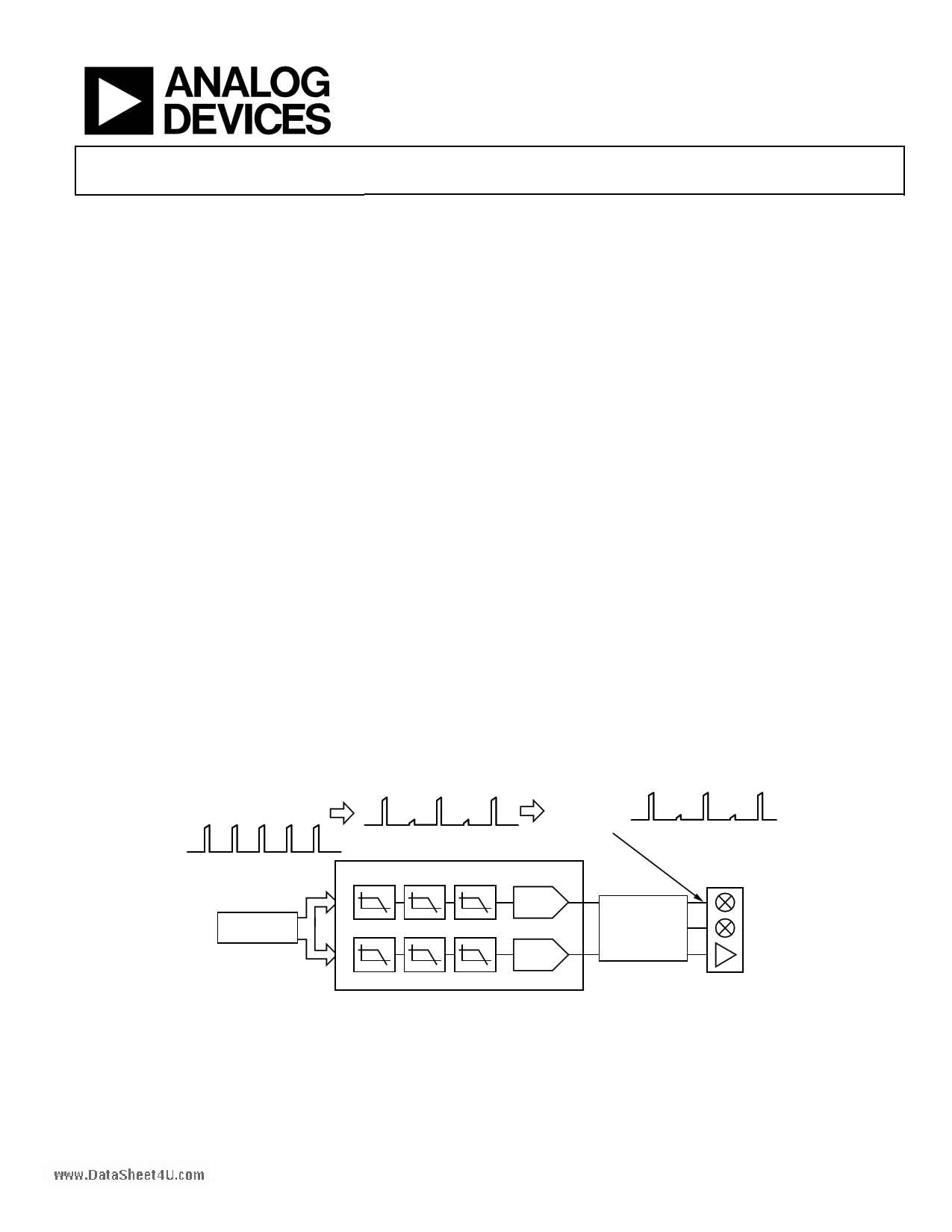
COMPLEX I AND Q
TYPICAL SIGNAL CHAIN
QUADRATURE
MODULATOR/
MIXER/
AMPLIFIER
DC
LO
DC
DIGITAL INTERPOLATION FILTERS
FPGA/ASIC/DSP
I DAC
Q DAC
POST DAC
ANALOG FILTER
A
AD9776A/AD9778A/AD9779A
Figure 1.
Rev. B
Information furnished by Analog Devices is believed to be accurate and reliable. However, no
responsibility is assumed by Analog Devices for its use, nor for any infringements of patents or other
rights of third parties that may result from its use. Specifications subject to change without notice. No
license is granted by implication or otherwise under any patent or patent rights of Analog Devices.
Trademarksandregisteredtrademarksarethepropertyoftheirrespectiveowners.
One Technology Way, P.O. Box 9106, Norwood, MA 02062-9106, U.S.A.
Tel: 781.329.4700
www.analog.com
Fax: 781.461.3113 ©2007–2008 Analog Devices, Inc. All rights reserved.
1 page 
AD9776A/wAwDw9.D7a7ta8ShAe/eAt4DU.c9o7m79A
SPECIFICATIONS
DC SPECIFICATIONS
TMIN to TMAX, AVDD33 = 3.3 V, DVDD33 = 3.3 V, DVDD18 = 1.8 V, CVDD18 = 1.8 V, IOUTFs = 20 mA, maximum sample rate, unless
otherwise noted.
Table 1.
Parameter
RESOLUTION
ACCURACY
Differential Nonlinearity (DNL)
Integral Nonlinearity (INL)
MAIN DAC OUTPUTS
Offset Error
Gain Error (with Internal Reference)
Full-Scale Output Current1
Output Compliance Range
Output Resistance
Gain DAC Monotonicity
MAIN DAC TEMPERATURE DRIFT
Offset
Gain
Reference Voltage
AUXILIARY DAC OUTPUTS
Resolution
Full-Scale Output Current1
Output Compliance Range (Source)
Output Compliance Range (Sink)
Output Resistance
Auxiliary DAC Monotonicity
REFERENCE
Internal Reference Voltage
Output Resistance
ANALOG SUPPLY VOLTAGES
AVDD33
CVDD18
DIGITAL SUPPLY VOLTAGES
DVDD33
DVDD18
POWER CONSUMPTION2
1× Mode, fDAC = 100 MSPS, IF = 1 MHz
2× Mode, fDAC = 320 MSPS, IF = 16 MHz, PLL Off
2× Mode, fDAC = 320 MSPS, IF = 16 MHz, PLL On
4× Mode, fDAC/4 Modulation, fDAC = 500 MSPS,
IF = 137.5 MHz, Q DAC Off
8× Mode, fDAC/4 Modulation, fDAC = 1 GSPS,
IF = 262.5 MHz
Power-Down Mode
Power Supply Rejection Ratio, AVDD33
OPERATING RANGE
AD9776A
Min Typ Max
12
AD9778A
Min Typ Max
14
AD9779A
Min Typ Max
16
Unit
Bits
±0.1
±0.86
±0.65
±1.5
±2.1 LSB
±6.0 LSB
−0.001 0
+0.001
±2
8.66 20.2 31.66
−1.0 +1.0
10
Guaranteed
−0.001 0
+0.001
±2
8.66 20.2 31.66
−1.0 +1.0
10
Guaranteed
−0.001 0
+0.001
±2
8.66 20.2 31.66
−1.0 +1.0
10
Guaranteed
% FSR
% FSR
mA
V
MΩ
0.04 0.04 0.04 ppm/°C
100 100 100 ppm/°C
30 30 30 ppm/°C
10
−1.998
+1.998
0 1.6
0.8 1.6
1
Guaranteed
10
−1.998
+1.998
0 1.6
0.8 1.6
1
Guaranteed
10
−1.998
+1.998
0 1.6
0.8 1.6
1
Guaranteed
Bits
mA
V
V
MΩ
1.2 1.2 1.2 V
5 5 5 kΩ
3.13 3.3 3.47 3.13 3.3 3.47 3.13 3.3 3.47 V
1.70 1.8 2.05 1.70 1.8 2.05 1.70 1.8 2.05 V
3.13 3.3 3.47 3.13 3.3 3.47 3.13 3.3 3.47 V
1.70 1.8 2.05 1.70 1.8 2.05 1.70 1.8 2.05 V
250 300
498
588
572
250 300
498
588
572
250 300
498
588
572
mW
mW
mW
mW
980 980 980 mW
2.5 9.8
2.5 9.8
2.5 9.8
mW
−0.3
+0.3 −0.3
+0.3 −0.3
+0.3 % FSR/V
−40 +25 +85 −40 +25 +85 −40 +25 +85 °C
1 Based on a 10 kΩ external resistor.
2 See the Power Dissipation section for more details.
Rev. B | Page 5 of 56
5 Page 
Pin
No. Mnemonic Description
33 DVDD18 1.8 V Digital Supply.
34 NC
No Connect.
35 NC
No Connect.
36 NC
No Connect.
37 DATACLK Data Clock Output.
38 DVDD33 3.3 V Digital Supply.
39 TXENABLE/ Transmit Enable. In single port mode, this
IQSELECT pin also functions as IQSELECT.
40 P2D11
Port 2, Data Input D11 (MSB).
41 P2D10
Port 2, Data Input D10.
42 P2D9
Port 2, Data Input D9.
43 DVDD18 1.8 V Digital Supply.
44 DGND
Digital Ground.
45 P2D8
Port 2, Data Input D8.
46 P2D7
Port 2, Data Input D7.
47 P2D6
Port 2, Data Input D6.
48 P2D5
Port 2, Data Input D5.
49 P2D4
Port 2, Data Input D4.
50 P2D3
Port 2, Data Input D3.
51 P2D2
Port 2, Data Input D2.
52 P2D1
Port 2, Data Input D1.
53 DVDD18 1.8 V Digital Supply.
54 DGND
Digital Ground.
55 P2D0
Port 2, Data Input D0 (LSB).
56 NC
No Connect.
57 NC
No Connect.
58 NC
No Connect.
59 NC
No Connect.
60 DVDD18 1.8 V Digital Supply.
61 DVDD33 3.3 V Digital Supply.
62 SYNC_O− Differential Synchronization Output.
63 SYNC_O+ Differential Synchronization Output.
64 DGND
Digital Ground.
65 PLL_LOCK PLL Lock Indicator.
66 SDO
3-Wire Interface Port Data Output.
67 SDIO
3-Wire Interface Port Data Input/Output.
68 SCLK
3-Wire Interface Port Clock.
AD9776A/wAwDw9.D7a7ta8ShAe/eAt4DU.c9o7m79A
Pin
No. Mnemonic Description
69 CSB
3-Wire Interface Port Chip Select Bar.
70 RESET
Reset, Active High.
71 IRQ
Interrupt Request.
72 AGND
Analog Ground.
73 IPTAT
Factory Test Pin. Output current is
proportional to absolute temperature,
approximately 14 μA at 25°C with
approximately 20 nA/°C slope. This pin
should remain floating.
74 VREF
Voltage Reference Output.
75 I120
120 μA Reference Current.
76 AVDD33 3.3 V Analog Supply.
77 AGND
Analog Ground.
78 AVDD33 3.3 V Analog Supply.
79 AGND
Analog Ground.
80 AVDD33 3.3 V Analog Supply.
81 AGND
Analog Ground.
82 AGND
Analog Ground.
83 OUT2_P Differential DAC Current Output, Channel 2.
84 OUT2_N Differential DAC Current Output, Channel 2.
85 AGND
Analog Ground.
86 AUX2_P Auxiliary DAC Current Output, Channel 2.
87 AUX2_N Auxiliary DAC Current Output, Channel 2.
88 AGND
Analog Ground.
89 AUX1_N Auxiliary DAC Current Output, Channel 1.
90 AUX1_P Auxiliary DAC Current Output, Channel 1.
91 AGND
Analog Ground.
92 OUT1_N Differential DAC Current Output, Channel 1.
93 OUT1_P Differential DAC Current Output, Channel 1.
94 AGND
Analog Ground.
95 AGND
Analog Ground.
96 AVDD33 3.3 V Analog Supply.
97 AGND
Analog Ground.
98 AVDD33 3.3 V Analog Supply.
99 AGND
Analog Ground.
100 AVDD33 3.3 V Analog Supply.
Rev. B | Page 11 of 56
11 Page | ||
| Páginas | Total 30 Páginas | |
| PDF Descargar | [ Datasheet AD9779A.PDF ] | |
Hoja de datos destacado
| Número de pieza | Descripción | Fabricantes |
| AD9779 | Digital-to-Analog Converters | Analog Devices |
| AD9779A | Dual 12-/14-/16-Bit 1 GSPS Digital-to-Analog Converters | Analog Devices |
| Número de pieza | Descripción | Fabricantes |
| SLA6805M | High Voltage 3 phase Motor Driver IC. |
Sanken |
| SDC1742 | 12- and 14-Bit Hybrid Synchro / Resolver-to-Digital Converters. |
Analog Devices |
|
DataSheet.es es una pagina web que funciona como un repositorio de manuales o hoja de datos de muchos de los productos más populares, |
| DataSheet.es | 2020 | Privacy Policy | Contacto | Buscar |