|
|
|
PDF ADG936 Data sheet ( Hoja de datos )
| Número de pieza | ADG936 | |
| Descripción | Wideband 4 GHz 36 dB Isolation at 1 GHz CMOS 1.65V to 2.75V Dual SPDT | |
| Fabricantes | Analog Devices | |
| Logotipo | ||
Hay una vista previa y un enlace de descarga de ADG936 (archivo pdf) en la parte inferior de esta página. Total 16 Páginas | ||
|
No Preview Available !
Wideband 4 GHz, 36 dB Isolation at 1 GHz,
www.DataSheet4U.com
CMOS 1.65 V to 2.75 V, Dual SPDT
ADG936/ADG936-R
FEATURES
Wideband switch: −3 dB @ 4 GHz
ADG936 absorptive dual SPDT
ADG936-R reflective dual SPDT
High off isolation (36 dB @ 1 GHz)
Low insertion loss (0.9 dB dc to 1 GHz)
Single 1.65 to 2.75 V power supply
CMOS/LVTTL control logic
20-lead TSSOP and 4 mm × 4 mm LFCSP package
Low power consumption (1 µA max)
APPLICATIONS
Wireless communications
General-purpose RF switching
Dual-band applications
High speed filter selection
Digital transceiver front end switch
IF switching
Tuner modules
Antenna diversity switching
GENERAL DESCRIPTION
The ADG936/ADG936-R are wideband analog switches that
comprise two independently selectable SPDT switches using a
CMOS process to provide high isolation and low insertion loss
to 1 GHz. The ADG936 is an absorptive/matched dual SPDT
with 50 Ω terminated shunt legs; the ADG936-R is a reflective
dual SPDT. These devices are designed such that the isolation is
high over the dc to 1 GHz frequency range. They have on-board
CMOS control logic, eliminating the need for external
controlling circuitry. The control inputs are both CMOS and
–10
VDD = 2.5V
TA = 25°C
–20
–30
–40
–50
S21
–60
–70 S12
–80
10k
100k
1M
10M
100M
FREQUENCY (Hz)
1G
Figure 3. Off Isolation vs. Frequency
10G
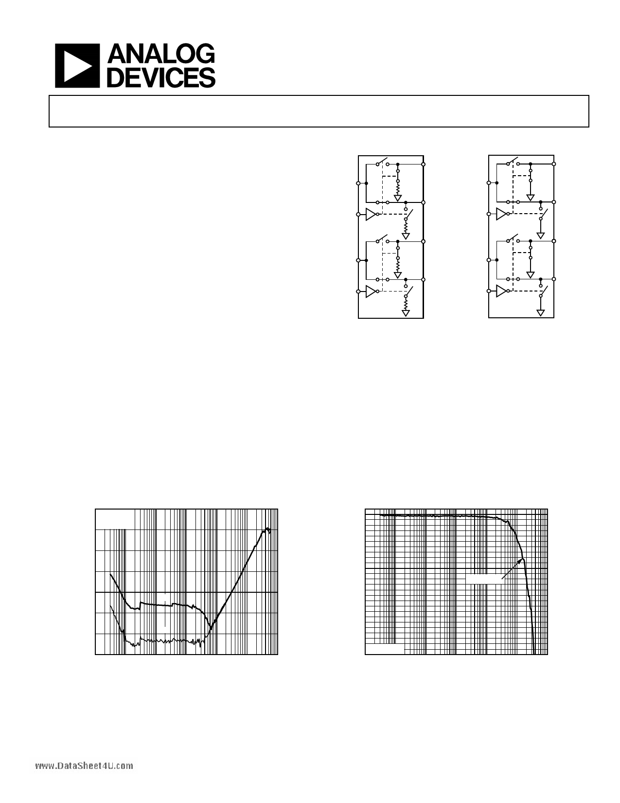
FUNCTIONAL BLOCK DIAGRAMS
RF1A
RFCA
50Ω
RF2A
INA
ADG936 50Ω
RF1B
RFCA
INA
ADG936-R
RFCB
INB
50Ω
RF2B
50Ω
RFCB
INB
RF1A
RF2A
RF1B
RF2B
Figure 1.
Figure 2.
LVTTL compatible. The low power consumption of these
CMOS devices makes them ideally suited for wireless
applications and general-purpose high frequency switching.
PRODUCT HIGHLIGHTS
1. –36 dB off isolation @ 1 GHz.
2. 0.9 dB insertion loss @ 1 GHz.
3. 20-lead TSSOP and 4 mm × 4 mm LFCSP package.
–0.3
–0.4
–0.5
–0.6
–0.7
–0.8
–0.9
–1.0
–1.1
–1.2
–1.3
–1.4
–1.5
–1.6
–1.7
–1.8
–1.9
–2.0
–2.1
–2.2
–2.3
–2.4
–2.5
–2.6
–2.7
–2.8
–2.9
–3.0
TA = 25°C
10k 100k
VDD = 2.5V
1M
10M
100M
FREQUENCY (Hz)
1G
10G
Figure 4. Insertion Loss vs. Frequency
Rev. 0
Information furnished by Analog Devices is believed to be accurate and reliable.
However, no responsibility is assumed by Analog Devices for its use, nor for any
infringements of patents or other rights of third parties that may result from its use.
Specifications subject to change without notice. No license is granted by implication
or otherwise under any patent or patent rights of Analog Devices. Trademarks and
registered trademarks are the property of their respective owners.
One Technology Way, P.O. Box 9106, Norwood, MA 02062-9106, U.S.A.
Tel: 781.329.4700
www.analog.com
Fax: 781.326.8703 © 2004 Analog Devices, Inc. All rights reserved.
1 page 
PIN CONFIGURATIONS AND FUNCTION DESCRIPTIONS
wAwDw.GDa9ta3S6he/AetD4UG.c9o3m6-R
RFCA 1
20 GND
VDD 2
19 INA
GND 3 ADG936 18 GND
RF1A 4 ADG936-R 17 RF2A
GND 5 TOP VIEW 16 GND
(Not to Scale)
GND 6
15 GND
RF1B 7
14 RF2B
GND 8
13 GND
GND 9
12 INB
RFCB 10
11 GND
Figure 5. 20-Lead TSSOP (RU-20)
GND 1
RF1A 2
GND 3
GND 4
RF1B 5
ADG936
ADG936-R
TOP VIEW
(Not to Scale)
15 GND
14 RF2A
13 GND
12 GND
11 RF2B
Figure 6. 20-Lead 4 mm × 4 mm LFCSP (CP-20)
Table 4. Pin Function Descriptions
Pin No.
20-Lead
TSSOP
20-Lead
LFCSP
Mnemonic
1 18 RFCA
2 19 VDD
3, 5, 6, 8, 9,
11,13, 15,
16, 18, 20
4
7
10
12
14
17
19
1, 3, 4, 6, 7,
9, 12,13, 15,
17, 20
2
5
8
10
11
14
16
GND
RF1A
RF1B
RFCB
INB
RF2B
RF2A
INA
Function
Common RF Port for Switch A.
Power Supply Input. These parts can be operated from 1.65 V to 2.75 V. VDD should be
decoupled to GND.
Ground Reference Point for All Circuitry on the Part.
RF1A Port.
RF1B Port.
Common RF Port for Switch B.
Logic Control Input.
RF2B Port.
RF2A Port.
Logic Control Input.
Rev. 0 | Page 5 of 16
5 Page 
APPLICATIONS
The ADG936/ADG936-R are ideal solutions for low power,
high frequency applications. The low insertion loss, high
isolation between ports, low distortion, and low current
consumption of these parts make them excellent solutions for
many high frequency switching applications. They can be used
in applications such as switchable filters, transmitters and
receivers for radar systems, and communication systems from
base stations to cell phones.
The ADG9xx family of wideband switches is designed to meet
the demands of devices transmitting at ISM band frequencies to
1 GHz and higher. The low insertion loss, high isolation
between ports, single pin control interface, no requirement for
dc blocking capacitors, and TTL interface compatibility make
them cost-effective and easy-to-integrate switching solutions for
many high frequency switching and low power applications,
because the parts can handle up to 16 dBm of power.
ABSORPTIVE VS. REFLECTIVE
The ADG936 is an absorptive (matched) switch with 50 Ω
terminated shunt legs; the ADG936-R is a reflective switch with
0 Ω terminated shunts to ground. The ADG936 absorptive
switch has a good VSWR on each port, regardless of the switch
mode. An absorptive switch should be used when there is a
need for a good VSWR that is looking into the port but not
passing the through-signal to the common port. The ADG936
is, therefore, ideal for applications that require minimum
reflections back to the RF source. It also ensures that the
maximum power is transferred to the load.
The ADG936-R reflective switch is suitable for applications in
which high off-port VSWR does not matter, and the switch has
some other desired performance features. It can be used in
many applications, including high speed filter selection. In most
cases, an absorptive switch can be used instead of a reflective
switch, but not vice versa.
wAwDw.GDa9ta3S6he/AetD4UG.c9o3m6-R
FILTER SELECTION
The ADG936 and ADG936-R can be used to switch high
frequency signals between different filters, and to multiplex the
signal to the output. These dual SPDT switches are also ideal for
high speed signal routing and for switching high speed
differential signals.
RF1A
RFIN
RFCA
RFIN
RFCB
ADG936
RF2A
RF1B
RF1A
RF2A
RF1B
ADG936
RFOUT
RFCA
RFOUT
RFCB
RF2B
RF2B
Figure 27. Filter Selection
Tx/Rx SWITCHING
The low insertion loss and high isolation between ports ensure
that the ADG936/ADG936-R are suitable transmit/receive
switches for all ISM band and Wireless LAN applications,
providing the required isolation between the transmit and
receive signals.
LNA
ANTENNA
RFCA
ADG936
RFCB
RF1B
PA
RF1B
RF2B
RF2B
Figure 28. Tx/Rx Switching
ANTENNA DIVERSITY SWITCH
The ADG936/ADG936-R are ideal for use as antenna diversity
switches, switching in different antennas to the tuner. The low
insertion loss, which ensures minimum signal loss and high
isolation between channels, makes these dual SPDT switches
suitable for switching applications in tuner modules and set-top
boxes.
Rev. 0 | Page 11 of 16
11 Page | ||
| Páginas | Total 16 Páginas | |
| PDF Descargar | [ Datasheet ADG936.PDF ] | |
Hoja de datos destacado
| Número de pieza | Descripción | Fabricantes |
| ADG936 | Wideband 4 GHz 36 dB Isolation at 1 GHz CMOS 1.65V to 2.75V Dual SPDT | Analog Devices |
| ADG936-R | Wideband 4 GHz 36 dB Isolation at 1 GHz CMOS 1.65V to 2.75V Dual SPDT | Analog Devices |
| Número de pieza | Descripción | Fabricantes |
| SLA6805M | High Voltage 3 phase Motor Driver IC. |
Sanken |
| SDC1742 | 12- and 14-Bit Hybrid Synchro / Resolver-to-Digital Converters. |
Analog Devices |
|
DataSheet.es es una pagina web que funciona como un repositorio de manuales o hoja de datos de muchos de los productos más populares, |
| DataSheet.es | 2020 | Privacy Policy | Contacto | Buscar |