|
|
|
PDF RMPA0959 Data sheet ( Hoja de datos )
| Número de pieza | RMPA0959 | |
| Descripción | CDMA and CDMA2000-1X PowerEdge Power Amplifier Module | |
| Fabricantes | Fairchild Semiconductor | |
| Logotipo | ||
Hay una vista previa y un enlace de descarga de RMPA0959 (archivo pdf) en la parte inferior de esta página. Total 13 Páginas | ||
|
No Preview Available !
www.DataSheet4U.com
March 2006
RMPA0959
CDMA and CDMA2000-1X PowerEdge™
Power Amplifier Module
Features
■ Single positive-supply operation with low power and shut-
down modes
■ 39% CDMA efficiency at +28dBm average output power
■ 53% AMPS mode efficiency at +31dBm output power
■ Lead-free RoHS compliant 4 x 4 x 1.5mm leadless
■ Internally matched to 50Ω and DC blocked RF input/output
■ Meets CDMA2000-1XRTT performance requirements
General Description
The RMPA0959 power amplifier module (PAM) is designed for
cellular band AMPS, CDMA and CDMA2000-1X applications.
The 2 stage PAM is internally matched to 50Ω to minimize the
use of external components and features a low-power mode to
reduce standby current and DC power consumption during peak
phone usage. High power-added efficiency and excellent linear-
ity are achieved using our Heterojunction Bipolar Transistor
(HBT) process.
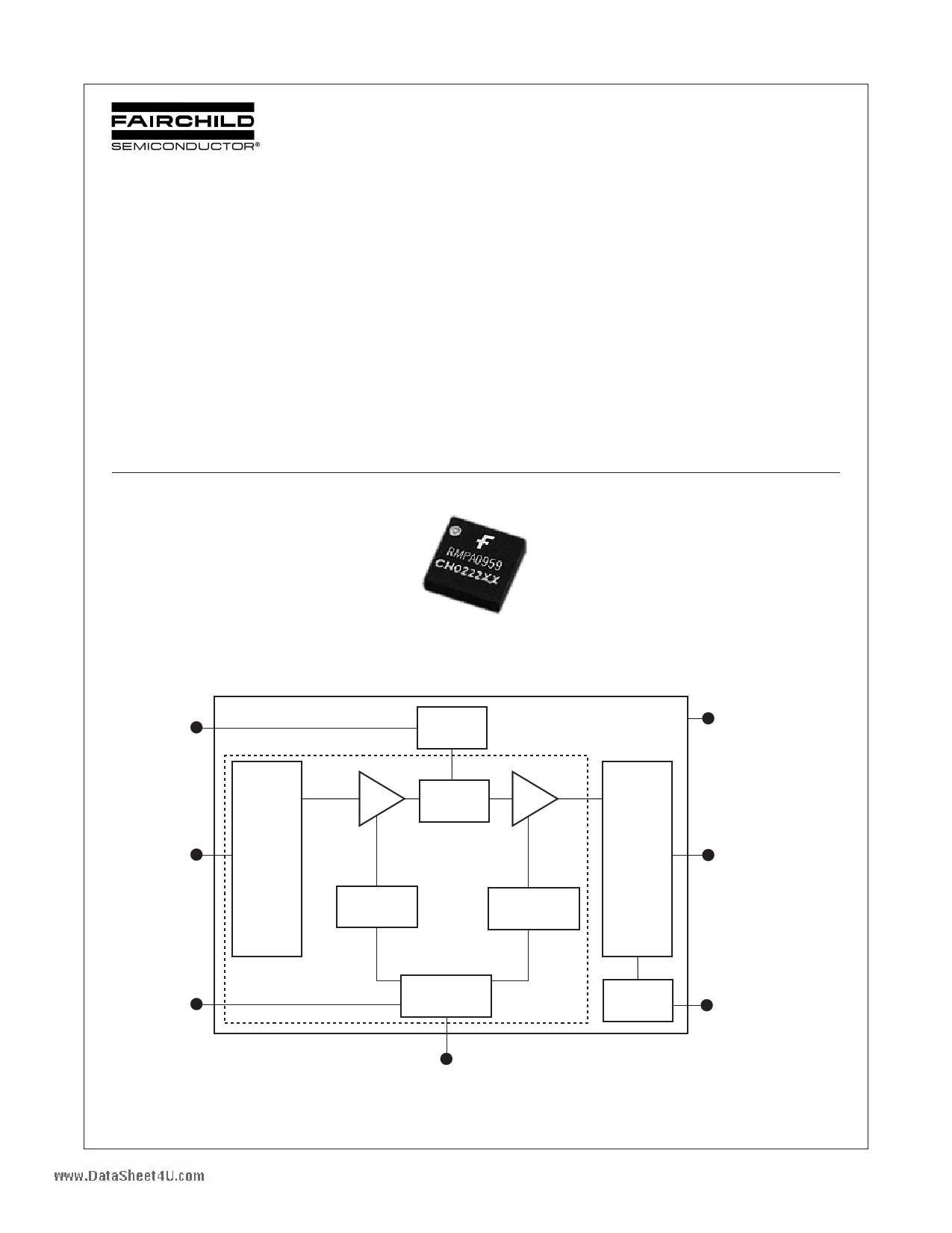
Device
Functional Block Diagram
Vcc1
(5)
PA MODULE
COLLECTOR
BIAS 1
GND
(3, 7, 9,10,11)
RF IN
(4)
Vref
(1)
INPUT
MATCHING
NETWORK
INTERSTAGE
MATCH
INPUT
STAGE MMIC
OUTPUT
STAGE
INPUT STAGE
BIAS
OUTPUT STAGE
BIAS
OUTPUT
MATCHING
NETWORK
RF OUT
(8)
VCC=3.4V (nom)
VREF=2.85V (nom)
824-849 MHz
50Ω I/O
BIAS CONTROL
COLLECTOR
BIAS 2
Vcc2
(6)
Vmode (2)
©2006 Fairchild Semiconductor Corporation
RMPA0959 Rev. F
1
www.fairchildsemi.com
1 page 
Typical Characteristics (Continued)
RMPA0959 Cellular 4x4 PAM, Pout = 16dBm, IS95 mod.
Vcc = 3.4V, Vref = 2.85V, Vmode = 2.0V, Tc = 25C,
-70.0
-72.0
-74.0
-76.0
-78.0
-80.0
824
836.5
Frequency (MHz)
849
www.DataSheet4U.com
500
450
400
350
300
250
200
150
100
50
0
0.0
RMPA0959 Cellular 4x4 PAM
Frequency = 836.5MHz, Vcc = 3.4V, Vref = 2.85V
Vmode = 0V
Vmode = 2.0V
4.0 8.0 12.0 16.0 20.0 24.0
Pout (dBm)
28.0
Efficiency Improvement Applications
In addition to high-power/low-power bias modes, the
efficiency of the PA module can be significantly increased
at backed-off RF power levels by dynamically varying the
supply voltage (Vcc) applied to the amplifier. Since mobile
handsets and power amplifiers frequently operate at 10-20
dB back-off, or more, from maximum rated linear power,
battery life is highly dependent on the DC power consumed
at antenna power levels in the range of 0 to +16dBm. The
reduced demand on transmitted RF power allows the PA
supply voltage to be reduced for improved efficiency, while
still meeting linearity requirements for CDMA modulation
with excellent margin. High-efficiency DC-DC converters
are now available to implement switched-voltage operation.
The following charts show measured performance of the
PA module in low-power mode (Vmode = +2.0V) at
+16dBm output power and over a range of supply voltages
from 3.4V nominal down to 1.5V over temp. Power-added
efficiency is more than doubled from 9.5 percent to nearly
20 percent (Vcc = 1.5V) while maintaining a typical ACPR1
of –52dBc and ACPR2 of less than –61dBc.
Operation at even lower levels of Vcc supply voltage are
possible with a further restriction on the maximum RF
output power. The PA module can be biased at a supply
voltage of as low as 0.7V with an efficiency as high as 10-
12 percent at +8dBm output power. Excellent signal
linearity is still maintained even under this low supply
voltage condition.
RMPA0959
Vref = 2.85V, Pout = 16dBm, Vmode = 2.0V
24.0
22.0
20.0
18.0
16.0
14.0
12.0
10.0
8.0
6.0
1.0 1.2 1.4 1.6 1.8 2.0 2.2 2.4 2.6 2.8 3.0 3.2 3.4 3.6
Vcc (V)
RMPA0959
Vref = 2.85V, Pout = 16dBm, Vmode = 2.0V
-40.0
-42.0
-44.0
-46.0
-48.0
-50.0
-52.0
-54.0
-56.0
1.0 1.2 1.4 1.6 1.8 2.0 2.2 2.4 2.6 2.8 3.0 3.2 3.4 3.6
Vcc (V)
RMPA0959
Vref = 2.85V, Pout = 16dBm, Vmode = 2.0V
30.0
28.0
26.0
24.0
22.0
20.0
1.0 1.2 1.4 1.6 1.8 2.0 2.2 2.4 2.6 2.8 3.0 3.2 3.4 3.6
Vcc (V)
-50.0
RMPA0959
Vref = 2.85V, Pout = 16dBm, Vmode = 2.0V
-55.0
-60.0
-65.0
-70.0
-75.0
-80.0
1.0 1.2 1.4 1.6 1.8 2.0 2.2 2.4 2.6 2.8 3.0 3.2 3.4 3.6
Vcc (V)
RMPA0959 Rev. F
5 www.fairchildsemi.com
5 Page 
www.DataSheet4U.com
Application Information
CAUTION: THIS IS AN ESD SENSITIVE DEVICE
Precautions to Avoid Permanent Device
Damage:
• Cleanliness: Observe proper handling procedures
to ensure clean devices and PCBs. Devices
should remain in their original packaging until
component placement to ensure no contamination
or damage to RF, DC & ground contact areas.
• Device Cleaning: Standard board cleaning
techniques should not present device problems
provided that the boards are properly dried to
remove solvents or water residues.
Solder Materials & Temperature Profile: Reflow
soldering is the preferred method of SMT
attachment. Hand soldering is not recommended.
• Reflow Profile
– Ramp-up: During this stage the solvents are
evaporated from the solder paste. Care should
be taken to prevent rapid oxidation (or paste
slump) and solder bursts caused by violent
solvent out-gassing. A typical heating rate is 1-
2°C/sec.
• Static Sensitivity: Follow ESD precautions to
protect against ESD damage:
– A properly grounded static-dissipative surface
on which to place devices.
– Static-dissipative floor or mat.
– A properly grounded conductive wrist strap for
each person to wear while handling devices.
• General Handling: Handle the package on the top
with a vacuum collet or along the edges with a
sharp pair of bent tweezers. Avoiding damaging
the RF, DC, & ground contacts on the package
bottom. Do not apply excessive pressure to the top
of the lid.
• Device Storage: Devices are supplied in heat-
sealed, moisture-barrier bags. In this condition,
devices are protected and require no special
storage conditions. Once the sealed bag has been
opened, devices should be stored in a dry nitrogen
environment.
Device Usage:
Fairchild recommends the following procedures prior
to assembly.
– Pre-heat/soak: The soak temperature stage
serves two purposes; the flux is activated and
the board and devices achieve a uniform
temperature. The recommended soak condition
is: 120-150 seconds at 150°C.
– Reflow Zone: If the temperature is too high, then
devices may be damaged by mechanical stress
due to thermal mismatch or there may be
problems due to excessive solder oxidation.
Excessive time at temperature can enhance the
formation of inter-metallic compounds at the
lead/board interface and may lead to early
mechanical failure of the joint. Reflow must
occur prior to the flux being completely driven
off. The duration of peak reflow temperature
should not exceed 10 seconds. Maximum
soldering temperatures should be in the range
215-220°C, with a maximum limit of 225°C.
– Cooling Zone: Steep thermal gradients may give
rise to excessive thermal shock. However, rapid
cooling promotes a finer grain structure and a
more crack-resistant solder joint. The illustration
below indicates the recommended soldering
profile.
• Dry-bake devices at 125°C for 24 hours minimum.
Note: The shipping trays cannot withstand 125°C
baking temperature.
• Assemble the dry-baked devices within 7 days of
removal from the oven.
Solder Joint Characteristics:
Proper operation of this device depends on a reliable
void-free attachment of the heatsink to the PWB. The
solder joint should be 95% void-free and be a
consistent thickness.
• During the 7-day period, the devices must be
stored in an environment of less than 60% relative
humidity and a maximum temperature of 30°C
• If the 7-day period or the environmental conditions
have been exceeded, then the dry-bake procedure
must be repeated.
Rework Considerations:
Rework of a device attached to a board is limited to
reflow of the solder with a heat gun. The device
should not be subjected to more than 225°C and
reflow solder in the molten state for more than 5
seconds. No more than 2 rework operations should
be performed.
RMPA0959 Rev. F
11 www.fairchildsemi.com
11 Page | ||
| Páginas | Total 13 Páginas | |
| PDF Descargar | [ Datasheet RMPA0959.PDF ] | |
Hoja de datos destacado
| Número de pieza | Descripción | Fabricantes |
| RMPA0951AT | 3V Cellular CDMA PowerEdge Power Amplifier Module | Fairchild Semiconductor |
| RMPA0959 | CDMA and CDMA2000-1X PowerEdge Power Amplifier Module | Fairchild Semiconductor |
| Número de pieza | Descripción | Fabricantes |
| SLA6805M | High Voltage 3 phase Motor Driver IC. |
Sanken |
| SDC1742 | 12- and 14-Bit Hybrid Synchro / Resolver-to-Digital Converters. |
Analog Devices |
|
DataSheet.es es una pagina web que funciona como un repositorio de manuales o hoja de datos de muchos de los productos más populares, |
| DataSheet.es | 2020 | Privacy Policy | Contacto | Buscar |