|
|
|
PDF NTP6410AN Data sheet ( Hoja de datos )
| Número de pieza | NTP6410AN | |
| Descripción | N-Channel Power MOSFET / Transistor | |
| Fabricantes | ON Semiconductor | |
| Logotipo | ||
Hay una vista previa y un enlace de descarga de NTP6410AN (archivo pdf) en la parte inferior de esta página. Total 7 Páginas | ||
|
No Preview Available !
NTB6410AN, NTP6410AN
N-Channel Power MOSFET
100 V, 76 A, 13 mW
Features
• Low RDS(on)
• High Current Capability
• 100% Avalanche Tested
• These are Pb−Free Devices
MAXIMUM RATINGS (TJ = 25°C Unless otherwise specified)
Parameter
Symbol Value
Drain−to−Source Voltage
Gate−to−Source Voltage − Continuous
Continuous Drain
Current RqJC
Steady
State
TC = 25°C
TC = 100°C
Power Dissipation
RqJC
Steady TC = 25°C
State
Pulsed Drain Current
tp = 10 ms
Operating Junction and Storage Temperature
Range
VDSS
VGS
ID
PD
IDM
TJ, Tstg
100
$20
76
54
188
305
−55 to
+175
Source Current (Body Diode)
Single Pulse Drain−to−Source Avalanche
Energy (VDD = 50 Vdc, VGS = 10 Vdc,
IL(pk) = 57.7 A, L = 0.3 mH, RG = 25 W)
Lead Temperature for Soldering
Purposes, 1/8″ from Case for 10 Seconds
IS 76
EAS 500
TL 260
Unit
V
V
A
W
A
°C
A
mJ
°C
THERMAL RESISTANCE RATINGS
www.DataSheet4U.com Parameter
Symbol Max Unit
Junction−to−Case (Drain) Steady State
RqJC
0.8 °C/W
Junction−to−Ambient (Note 1)
RqJA
32
Stresses exceeding Maximum Ratings may damage the device. Maximum
Ratings are stress ratings only. Functional operation above the Recommended
Operating Conditions is not implied. Extended exposure to stresses above the
Recommended Operating Conditions may affect device reliability.
1. Surface mounted on FR4 board using 1 sq in pad size,
(Cu Area 1.127 sq in [2 oz] including traces).
© Semiconductor Components Industries, LLC, 2009
December, 2009 − Rev. 0
1
http://onsemi.com
V(BR)DSS
100 V
RDS(ON) MAX
13 mW @ 10 V
ID MAX
(Note 1)
76 A
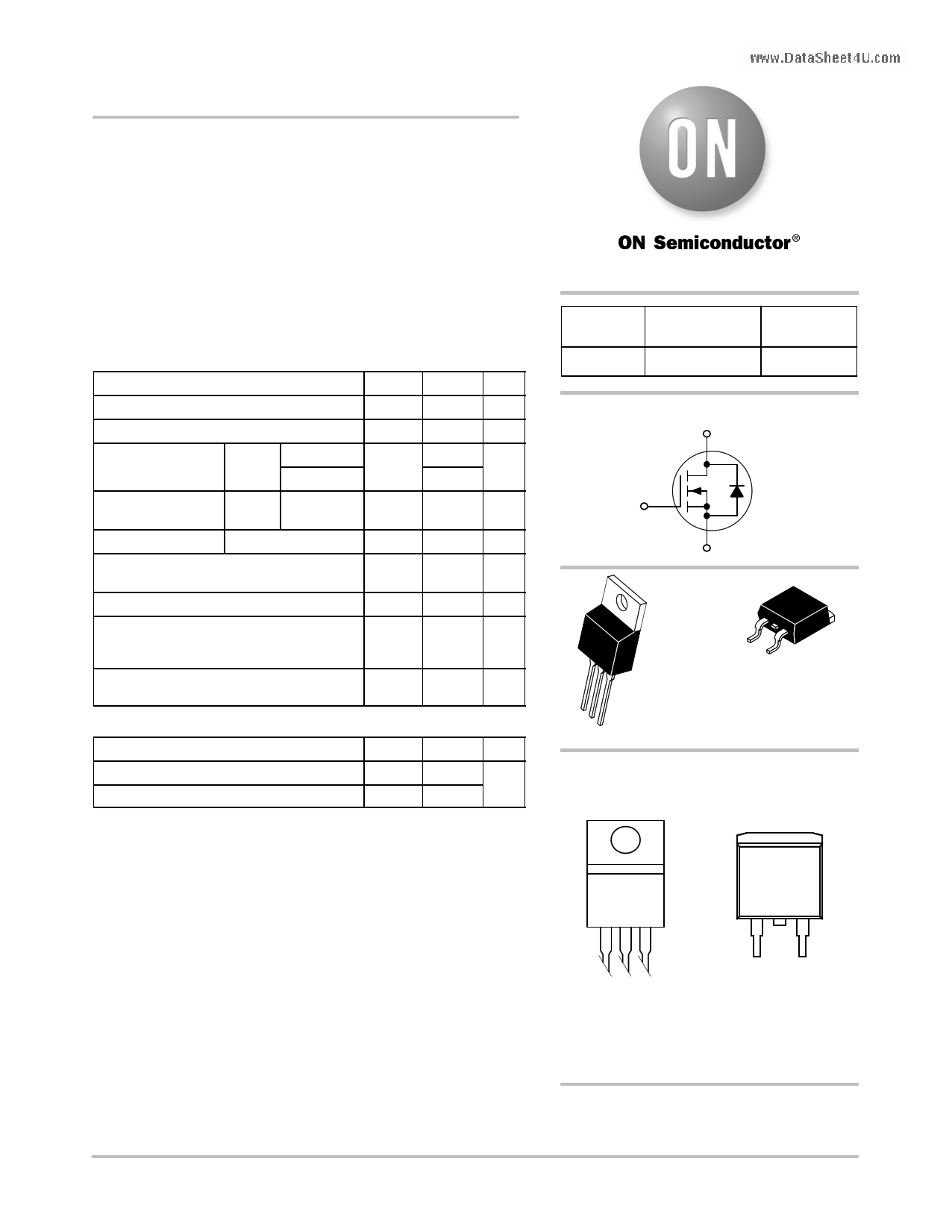
N−Channel
D
G
S
4
4
12
3
TO−220AB
CASE 221A
STYLE 5
12
3
D2PAK
CASE 418B
STYLE 2
MARKING DIAGRAM
& PIN ASSIGNMENT
4
Drain
4
Drain
NTP
6410ANG
AYWW
1
Gate
3
Source
NTB
6410ANG
AYWW
1
Gate
2
Drain
3
Source
2
Drain
6410AN = Specific Device Code
G = Pb−Free Device
A = Assembly Location
Y = Year
WW = Work Week
ORDERING INFORMATION
See detailed ordering and shipping information in the package
dimensions section on page 5 of this data sheet.
Publication Order Number:
NTB6410AN/D
1 page 
1
D = 0.5
0.2
0.1 0.1
0.05
0.02
0.01 0.01 SINGLE PULSE
NTB6410AN, NTP6410AN
0.001
0.000001 0.00001
0.0001
0.001
0.01
0.1
1.0
10
100 1000
t, PULSE TIME (s)
Figure 13. Thermal Response
ORDERING INFORMATION
Device
NTB6410ANG
Package
D2PAK
(Pb−Free)
Shipping†
50 Units / Rail
NTB6410ANT4G
D2PAK
(Pb−Free)
800 / Tape & Reel
NTP6410ANG
TO−220
(Pb−Free)
50 Units / Rail
†For information on tape and reel specifications, including part orientation and tape sizes, please refer to our Tape and Reel Packaging
Specifications Brochure, BRD8011/D.
www.DataSheet4U.com
http://onsemi.com
5
5 Page | ||
| Páginas | Total 7 Páginas | |
| PDF Descargar | [ Datasheet NTP6410AN.PDF ] | |
Hoja de datos destacado
| Número de pieza | Descripción | Fabricantes |
| NTP6410AN | N-Channel Power MOSFET / Transistor | ON Semiconductor |
| Número de pieza | Descripción | Fabricantes |
| SLA6805M | High Voltage 3 phase Motor Driver IC. |
Sanken |
| SDC1742 | 12- and 14-Bit Hybrid Synchro / Resolver-to-Digital Converters. |
Analog Devices |
|
DataSheet.es es una pagina web que funciona como un repositorio de manuales o hoja de datos de muchos de los productos más populares, |
| DataSheet.es | 2020 | Privacy Policy | Contacto | Buscar |