|
|
|
PDF AD7944 Data sheet ( Hoja de datos )
| Número de pieza | AD7944 | |
| Descripción | PulSAR 15.5 mW ADC | |
| Fabricantes | Analog Devices | |
| Logotipo | ||
Hay una vista previa y un enlace de descarga de AD7944 (archivo pdf) en la parte inferior de esta página. Total 28 Páginas | ||
|
No Preview Available !
14-Bit, 2.5 MSPS, PulSAR
15.5 mW ADC in LFCSP
AD7944
FEATURES
14-bit resolution with no missing codes
Throughput: 2.5 MSPS (TURBO high), 2.0 MSPS (TURBO low)
Low power dissipation
15.5 mW at 2.5 MSPS, with external reference
28 mW at 2.5 MSPS, with internal reference
INL: ±0.25 LSB typical, ±1.0 LSB maximum
SNR
84 dB, with on-chip reference
84.5 dB, with external reference
4.096 V internal reference: typical drift of ±10 ppm/°C
Pseudo differential analog input voltage range
0 V to VREF with VREF up to 5.0 V
Allows use of any input range
No pipeline delay
Logic interface: 1.8 V/2.5 V/2.7 V
Serial interface: SPI-/QSPI-/MICROWIRE-/DSP-compatible
Ability to daisy-chain multiple ADCs with busy indicator
20-lead, 4 mm × 4 mm LFCSP (QFN)
APPLICATIONS
Battery-powered equipment
Communications
ATE
Data acquisition systems
Medical instruments
www.DataSheet4U.com
0V
TO
VREF
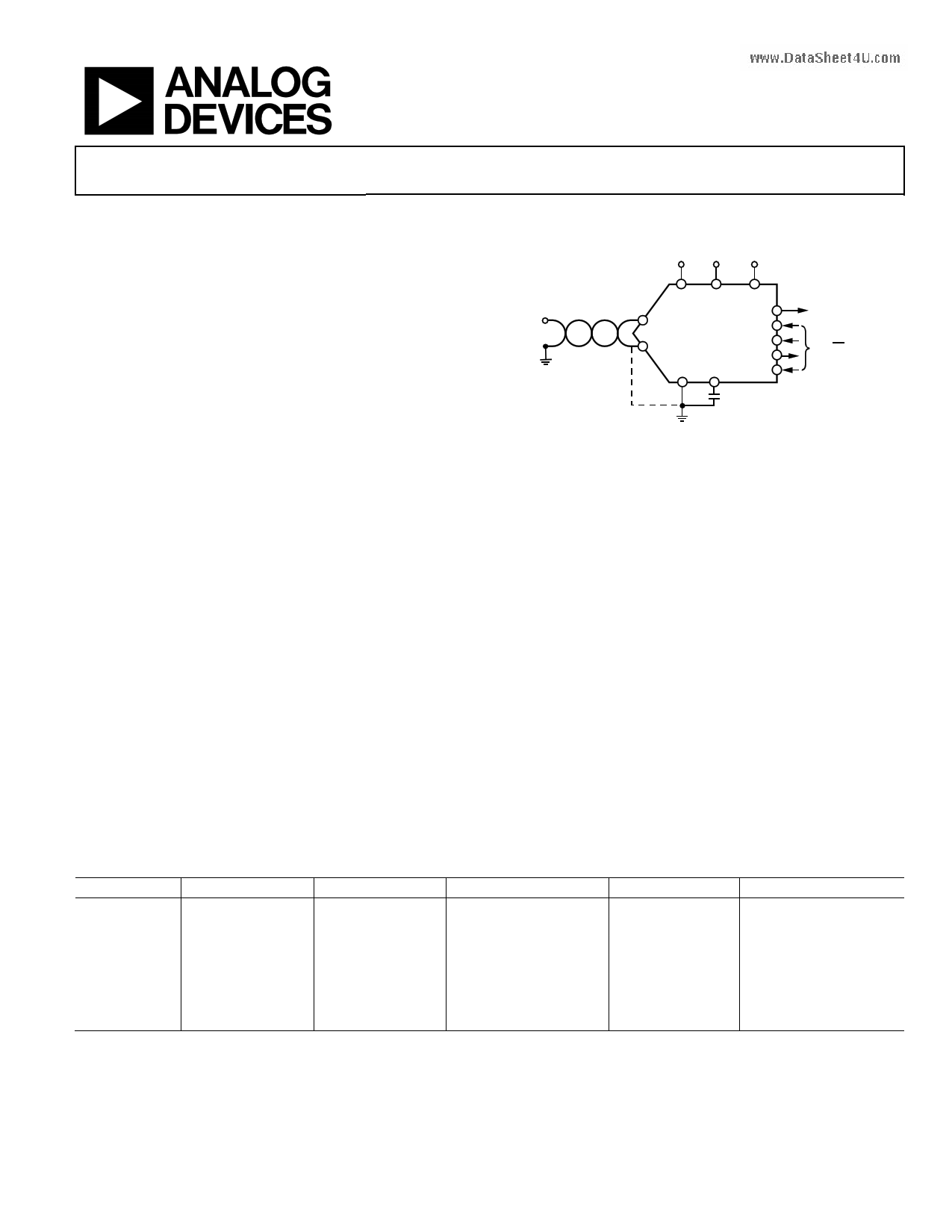
APPLICATION DIAGRAM
1.8V
TO
5V 2.5V 2.7V
BVDD AVDD, VIO
DVDD TURBO
IN+ SDI
AD7944
IN–
SCK
SDO
GND REF
CNV
10µF
VIO
3- OR 4-WIRE
INTERFACE:
SPI, CS,
DAISY CHAIN
(TURBO = LOW)
NOTES
1. GND REFERS TO REFGND, AGND, AND DGND.
Figure 1.
GENERAL DESCRIPTION
The AD7944 is a 14-bit, 2.5 MSPS successive approximation
analog-to-digital converter (SAR ADC). It contains a low power,
high speed, 14-bit sampling ADC, an internal conversion clock,
an internal reference (and buffer), error correction circuits, and
a versatile serial interface port. On the rising edge of CNV, the
AD7944 samples an analog input, IN+, between 0 V and VREF
with respect to a ground sense, IN−. The AD7944 features a
very high sampling rate turbo mode (TURBO high) and a
reduced power normal mode (TURBO low) for low power
applications where the power is scaled with the throughput.
In normal mode (TURBO low), the SPI-compatible serial inter-
face also features the ability, using the SDI input, to daisy-chain
several ADCs on a single 3-wire bus and provide an optional busy
indicator. The serial interface is compatible with 1.8 V, 2.5 V,
and 2.7 V supplies using the separate VIO supply.
The AD7944 is available in a 20-lead LFCSP with operation
specified from −40°C to +85°C.
Table 1. MSOP, LFCSP, 14-/16-/18-Bit PulSAR® ADCs1
Type
100 kSPS
250 kSPS
14-Bit
AD7940
AD79422
16-Bit
AD7680
AD76852
AD7683
AD76872
AD7684
AD7694
18-Bit
AD76912
400 kSPS to 500 kSPS
AD79462
AD76862
AD76882
AD76932
AD76902
≥1000 kSPS
AD79443
AD79802
AD79832
AD79853
AD79822
AD79842
AD79863
ADC Driver
ADA4941-1
ADA4841-x
AD8021
ADA4941-1
ADA4841-x
AD8021
1 See www.analog.com for the latest selection of PulSAR ADCs and ADC drivers.
2 Pin-for-pin compatible with all other parts marked with this endnote.
3 The AD7944, AD7985, and AD7986 are pin-for-pin compatible.
Rev. 0
Information furnished by Analog Devices is believed to be accurate and reliable. However, no
responsibility is assumed by Analog Devices for its use, nor for any infringements of patents or other
rights of third parties that may result from its use. Specifications subject to change without notice. No
license is granted by implication or otherwise under any patent or patent rights of Analog Devices.
Trademarksandregisteredtrademarksarethepropertyoftheirrespectiveowners.
One Technology Way, P.O. Box 9106, Norwood, MA 02062-9106, U.S.A.
Tel: 781.329.4700
www.analog.com
Fax: 781.461.3113
©2009 Analog Devices, Inc. All rights reserved.
1 page 
AD7944
TIMING SPECIFICATIONS
AVDD = DVDD = 2.5 V, BVDD = 5 V, VIO = 1.8 V to 2.7 V, VREF = 4.096 V, TA = −40°C to +85°C, unless otherwise noted.1
Table 4.
Parameter
Conversion Time: CNV Rising Edge
to Data Available
Acquisition Time
Time Between Conversions
CNV Pulse Width
Data Read During Conversion
Quiet Time During Acquisition from Last SCK
Falling Edge to CNV Rising Edge
SCK Period
SCK Low Time
SCK High Time
SCK Falling Edge to Data Remains Valid
SCK Falling Edge to Data Valid Delay
CNV or SDI Low to SDO D13 MSB Valid
CNV or SDI High or Last SCK Falling Edge
to SDO High Impedance
SDI Valid Setup Time from CNV Rising Edge
SDI Valid Hold Time from CNV Rising Edge
SCK Valid Setup Time from CNV Rising Edge
SCK Valid Hold Time from CNV Rising Edge
SDI Valid Setup Time from SCK Falling Edge
SDI Valid Hold Time from SCK Falling Edge
SDI High to SDO High
www.DataSheet4U.com
1 See Figure 2 and Figure 3 for load conditions.
Symbol
tCONV
tCONV
tACQ
tCYC
tCYC
tCNVH
tDATA
tDATA
tQUIET
tSCK
tSCK
tSCKL
tSCKH
tHSDO
tDSDO
tEN
tDIS
tSSDICNV
tHSDICNV
tHSDICNV
tSSCKCNV
tHSCKCNV
tSSDISCK
tHSDISCK
tDSDOSDI
Test Conditions/Comments
Turbo mode
Normal mode
Turbo mode
Normal mode
CS mode
Turbo mode
Normal mode
CS mode
Chain mode
Min
320
420
80
400
500
10
20
9
11
3.5
3.5
2
CS mode
CS mode
Chain mode
Chain mode
Chain mode
Chain mode
Chain mode
Chain mode with busy indicator
4
0
0
5
5
2
3
Typ Max
190
290
4
5
8
15
Unit
ns
ns
ns
ns
ns
ns
ns
ns
ns
ns
ns
ns
ns
ns
ns
ns
ns
ns
ns
ns
ns
ns
ns
ns
ns
500µA IOL
TO SDO
CL
20pF
1.4V
500µA IOH
Figure 2. Load Circuit for Digital Interface Timing
90% VIO
tDELAY
VIH1
VIL1
10% VIO
tDELAY
VIH1
VIL1
1MINIMUM VIH AND MAXIMUM VIL USED. SEE DIGITAL INPUTS
SPECIFICATIONS IN TABLE 3.
Figure 3. Voltage Levels for Timing
Rev. 0 | Page 5 of 28
5 Page 
90
89
88
87
86
85
84
83
82
81
80
–10 –9 –8 –7 –6 –5 –4 –3 –2 –1
INPUT LEVEL (dBFS)
Figure 17. SNR vs. Input Level
0
2.0
1.8 IAVDD
1.6
IDVDD
1.4
1.2 IVIO
1.0
0.8
IBVDD
0.6
IREF
0.4
0.2
0
2.375
2.425
2.475
2.525
2.575
AVDD AND DVDD VOLTAGE (V)
Figure 18. Operating Current vs. Supply Voltage
www.DataSheet4U.com
2.625
AD7944
2.0
1.8
1.6 IAVDD
1.4
1.2
1.0
0.8
IBVDD
0.6
IREF
0.4
0.2
0
–55 –35 –15
5 25 45 65
TEMPERATURE (°C)
85 105 125
Figure 19. Operating Current vs. Temperature
14
12
10
8
6
4
IAVDD + IDVDD + IVIO
2
0
–55 –35 –15
5 25 45 65
TEMPERATURE (°C)
85 105
Figure 20. Power-Down Current vs. Temperature
125
Rev. 0 | Page 11 of 28
11 Page | ||
| Páginas | Total 28 Páginas | |
| PDF Descargar | [ Datasheet AD7944.PDF ] | |
Hoja de datos destacado
| Número de pieza | Descripción | Fabricantes |
| AD7940 | 14-Bit ADC | Analog Devices |
| AD7942 | PulSAR ADC | Analog Devices |
| AD7943 | +3.3 V/+5 V Multiplying 12-Bit DACs | Analog Devices |
| AD7944 | PulSAR 15.5 mW ADC | Analog Devices |
| Número de pieza | Descripción | Fabricantes |
| SLA6805M | High Voltage 3 phase Motor Driver IC. |
Sanken |
| SDC1742 | 12- and 14-Bit Hybrid Synchro / Resolver-to-Digital Converters. |
Analog Devices |
|
DataSheet.es es una pagina web que funciona como un repositorio de manuales o hoja de datos de muchos de los productos más populares, |
| DataSheet.es | 2020 | Privacy Policy | Contacto | Buscar |