|
|
|
PDF ADG1414 Data sheet ( Hoja de datos )
| Número de pieza | ADG1414 | |
| Descripción | Serially-Controlled Octal SPST Switches | |
| Fabricantes | Analog Devices | |
| Logotipo | ||
Hay una vista previa y un enlace de descarga de ADG1414 (archivo pdf) en la parte inferior de esta página. Total 20 Páginas | ||
|
No Preview Available !
9.5 Ω RON ±15 V/+12 V/±5 V iCMOS
Serially-Controlled Octal SPST Switches
ADG1414
FEATURES
SPI interface
Supports daisy-chain mode
9.5 Ω on resistance @ 25°C
1.6 Ω on-resistance flatness
Fully specified at ±15 V, +12 V, ±5 V
3 V logic-compatible inputs
Rail-to-rail operation
24-lead TSSOP and 24-lead 4 mm × 4 mm LFCSP
APPLICATIONS
Automatic test equipment
Data acquisition systems
Battery-powered systems
Sample-and-hold systems
Audio signal routing
Video signal routing
Communication systems
GENERAL DESCRIPTION
The ADG1414 is a monolithic complementary metal-oxide
semiconductor (CMOS) device containing eight independently
selectable switches designed on an industrial CMOS (iCMOS®)
process. iCMOS is a modular manufacturing process combining
high voltage CMOS and bipolar technologies. iCMOS components
can tolerate high supply voltages while providing increased perfor-
mance, dramatically lower power consumption, and reduce the
package size.
www.DataSheet4U.com
The ADG1414 is a set of octal SPST (single-pole, single-throw)
switches controlled via a 3-wire serial interface. On resistance is
closely matched between switches and is very flat over the full
signal range. Each switch conducts equally well in both direc-
tions and the input signal range extends to the supplies.
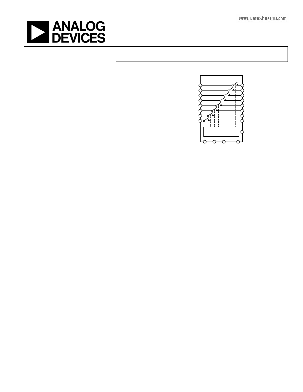
FUNCTIONAL BLOCK DIAGRAM
ADG1414
S1 D1
S2 D2
S3 D3
S4 D4
S5 D5
S6 D6
S7 D7
S8 D8
INPUT SHIFT
REGISTER
SDO
SCLK DIN SYNC RESET/VL
Figure 1.
Data is written to these devices in the form of eight bits; each
bit corresponds to one channel.
The ADG1414 utilizes a versatile 3-wire serial interface that
operates at clock rates of up to 50 MHz and is compatible with
standard SPI, QSPI™, MICROWIRE™, and DSP interface
standards. The output of the shift register, SDO, enables a
number of these parts to be daisy chained.
On power-up, all switches are in the off condition, and the
internal registers contain all zeros.
PRODUCT HIGHLIGHTS
1. 50 MHz serial interface.
2. 9.5 Ω on resistance.
3. 1.6 Ω on-resistance flatness.
4. 24-lead TSSOP and 4 mm × 4 mm LFCSP packages.
Rev. 0
Information furnished by Analog Devices is believed to be accurate and reliable. However, no
responsibilityisassumedbyAnalog Devicesforitsuse,norforanyinfringementsofpatentsorother
rights of third parties that may result from its use. Specifications subject to change without notice. No
license is granted by implication or otherwise under any patent or patent rights of Analog Devices.
Trademarks and registered trademarks are the property of their respective owners.
One Technology Way, P.O. Box 9106, Norwood, MA 02062-9106, U.S.A.
Tel: 781.329.4700
www.analog.com
Fax: 781.461.3113
©2009 Analog Devices, Inc. All rights reserved.
1 page 
Parameter
LOGIC OUTPUTS (SDO)
VOL, Output Low Voltage1
−40°C to
+25°C +85°C
High Impedance Leakage Current
High Impedance Output
Capacitance1
DYNAMIC CHARACTERISTICS1
tON
tOFF
Charge Injection
4
145
185
35
45
8
220
46
Off Isolation
−70
Channel-to-Channel Crosstalk
−75
−3 dB Bandwidth
Insertion Loss
240
1.15
CD, CS (Off )
CD, CS (On)
POWER REQUIREMENTS
IDD
12
33
0.001
IL Inactive
0.3
IL Active @ 30 MHz
www.DataILSAhceteivt4eU@.co5m0 MHz
ISS
0.26
0.3
0.42
0.5
0.001
VDD/VSS
1 Guaranteed by design, not subject to production test.
−40°C to
+125°C
0.4
0.6
±1
240
46
1
1
0.35
0.55
1
±4.5/±16.5
ADG1414
Unit
V max
V max
μA max
pF typ
Test Conditions/Comments
ISINK = 3 mA
ISINK = 6 mA
ns typ
ns max
ns typ
ns max
pC typ
dB typ
dB typ
MHz typ
dB typ
pF typ
pF typ
μA typ
μA max
μA typ
μA max
mA typ
mA max
mA typ
mA max
μA typ
μA max
V min/max
RL = 100 Ω, CL = 35 pF
VS = 8 V; see Figure 30
RL = 100 Ω, CL = 35 pF
VS = 8 V; see Figure 30
VS = 6 V, RS = 0 Ω, CL = 1 nF; see
Figure 31
RL = 50 Ω, CL = 5 pF, f = 1 MHz;
see Figure 26
RL = 50 Ω, CL = 5 pF, f = 1 MHz;
see Figure 27
RL = 50 Ω, CL = 5 pF; see Figure 28
RL = 50 Ω, CL = 5 pF, f = 1 MHz; see
Figure 28
f = 1 MHz
f = 1 MHz
VDD = +13.2 V
Digital inputs = 0 V or VL
Digital inputs = 0 V or VL
Digital inputs toggle between 0 V
and VL
Digital inputs toggle between 0V
and VL
Digital inputs = 0 V or VL
Rev. 0 | Page 5 of 20
5 Page 
ADG1414
PIN CONFIGURATIONS AND FUNCTION DESCRIPTIONS
SCLK 1
24 SYNC
VDD 2
DIN 3
23 RESET/VL
22 SDO
GND 4
S1 5
D1 6
S2 7
ADG1414
TOP VIEW
(Not to Scale)
21 VSS
20 S8
19 D8
18 S7
D2 8
17 D7
S3 9
16 S6
D3 10
15 D6
S4 11
14 S5
D4 12
13 D5
GND 1
S1 2
D1 3
S2 4
D2 5
S3 6
PIN 1
INDICATOR
ADG1414
TOP VIEW
(Not to Scale)
18 VSS
17 S8
16 D8
15 S7
14 D7
13 S6
NOTES
1. EXPOSED PAD TIED TO SUBSTRATE, VSS.
Figure 4. TSSOP Pin Configuration
Figure 5. LFCSP Pin Configuration
Table 9. Pin Function Descriptions
Pin No.
TSSOP LFCSP
Mnemonic
1 22
SCLK
2 23
3 24
VDD
DIN
41
52
63
74
85
96
www.Da1t0aSheet4U7.com
11 8
12 9
13 10
14 11
15 12
16 13
17 14
18 15
19 16
20 17
21 18
GND
S1
D1
S2
D2
S3
D3
S4
D4
D5
S5
D6
S6
D7
S7
D8
S8
VSS
22 19
SDO
23 20
RESET/VL
Description
Serial Clock Input. Data is clocked into the input shift register on the falling edge of the serial
clock input. Data can be transferred at rates of up to 50 MHz.
Most Positive Power Supply Potential.
Serial Data Input. This device has an 8-bit shift register. Data is clocked into the register on the
falling edge of the serial clock input.
Ground (0 V) Reference.
Source Terminal 1. This pin can be an input or an output.
Drain Terminal 1. This pin can be an input or an output.
Source Terminal 2. This pin can be an input or an output.
Drain Terminal 2. This pin can be an input or an output.
Source Terminal 3. This pin can be an input or an output.
Drain Terminal 3. This pin can be an input or an output.
Source Terminal 4. This pin can be an input or an output.
Drain Terminal 4. This pin can be an input or an output.
Drain Terminal 5. This pin can be an input or an output.
Source Terminal 5. This pin can be an input or an output.
Drain Terminal 6. This pin can be an input or an output.
Source Terminal 6. This pin can be an input or an output.
Drain Terminal 7. This pin can be an input or an output.
Source Terminal 7. This pin can be an input or an output.
Drain Terminal 8. This pin can be an input or an output.
Source Terminal 8. This pin can be an input or an output.
Most Negative Power Supply Potential. In single-supply applications, it can be connected to
ground.
Serial Data Output. This pin can be used for daisy-chaining a number of these devices together or
for reading back the data in the shift register for diagnostic purposes. The serial data is transferred
on the rising edge of SCLK and is valid on the falling edge of the clock. Pull this open-drain output
to the supply with an external resistor.
RESET/Logic Power Supply Input (VL). When this pin is low (<0.8 V), this pin acts as RESET, all
switches are open, and appropriate registers are cleared to 0. Otherwise, it is the logic power
supply input that operates from 2.7 V to 5.5 V.
Rev. 0 | Page 11 of 20
11 Page | ||
| Páginas | Total 20 Páginas | |
| PDF Descargar | [ Datasheet ADG1414.PDF ] | |
Hoja de datos destacado
| Número de pieza | Descripción | Fabricantes |
| ADG1411 | (ADG1411 - ADG1413) Quad SPST Switch | Analog Devices |
| ADG1412 | (ADG1411 - ADG1413) Quad SPST Switch | Analog Devices |
| ADG1413 | (ADG1411 - ADG1413) Quad SPST Switch | Analog Devices |
| ADG1414 | Serially-Controlled Octal SPST Switches | Analog Devices |
| Número de pieza | Descripción | Fabricantes |
| SLA6805M | High Voltage 3 phase Motor Driver IC. |
Sanken |
| SDC1742 | 12- and 14-Bit Hybrid Synchro / Resolver-to-Digital Converters. |
Analog Devices |
|
DataSheet.es es una pagina web que funciona como un repositorio de manuales o hoja de datos de muchos de los productos más populares, |
| DataSheet.es | 2020 | Privacy Policy | Contacto | Buscar |