|
|
|
PDF ADA4420-6 Data sheet ( Hoja de datos )
| Número de pieza | ADA4420-6 | |
| Descripción | Low Cost 6-Channel HD/SD Video Filter | |
| Fabricantes | Analog Devices | |
| Logotipo | ||
Hay una vista previa y un enlace de descarga de ADA4420-6 (archivo pdf) en la parte inferior de esta página. Total 17 Páginas | ||
|
No Preview Available !
Low Cost 6-Channel HD/SD Video Filter
ADA4420-6
FEATURES
Sixth-order filters
Transparent input sync tip clamp
−1 dB bandwidth of 26 MHz typical for HD
HD rejection @ 75 MHz: 48 dB typical
NTSC differential gain: 0.19%
NTSC differential phase: 0.76°
Rail-to-rail outputs
Low quiescent current: 32 mA typical
Disable feature
Output dc offset
APPLICATIONS
Set-top boxes
DVD players and recorders
HDTVs
Projectors
Personal video recorders
GENERAL DESCRIPTION
The ADA4420-6 is a low cost video reconstruction filter specifically
designed for consumer applications. It consists of six independent
sixth-order Butterworth filters/buffers, three for standard
definition (Y/C or CVBS) and three for high definition
component signals (YPrPb or RGB).
The ADA4420-6 operates from a single 5 V supply and has a
low quiescent current of 32 mA, making it ideal for applications
where power consumption is critical. A disable feature allows
for further power conservation by reducing the supply current
to less than 8 μA typical when the device is not in use.
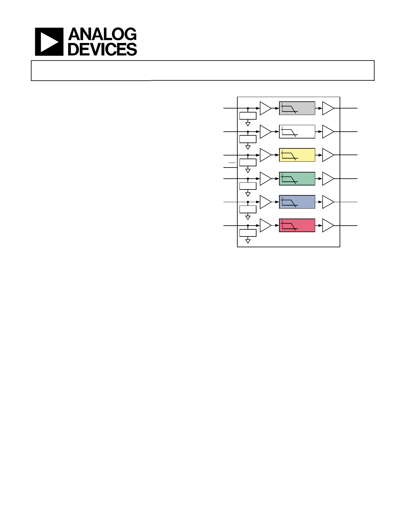
FUNCTIONAL BLOCK DIAGRAM
INSD1
CLAMP
×1
INSD2
CLAMP
×1
INSD3
DIS CLAMP
×1
INHD1
CLAMP
×1
INHD2
CLAMP
×1
SD ×2 OUTSD1
OUTSD2
SD ×2
OUTSD3
SD ×2
HD ×2 OUTHD1
OUTHD2
HD ×2
INHD3
CLAMP
×1
OUTHD3
HD ×2
ADA4420-6
Figure 1.
Each channel features a transparent sync tip clamp, allowing ac
coupling of the inputs without requiring dc restoration.
The output drivers on the ADA4420-6 have rail-to-rail output
capabilities with 6 dB gain. A built-in offset of 250 mV allows
the outputs to be dc-coupled, eliminating the need for large
coupling capacitors. Each output is capable of driving two 75 Ω
doubly terminated cables.
The ADA4420-6 is available in either a 16-lead QSOP or a 20-lead
TSSOP, and operates in the extended industrial temperature
range of −40°C to +85°C.
Rev. A
Information furnished by Analog Devices is believed to be accurate and reliable. However, no
responsibility is assumed by Analog Devices for its use, nor for any infringements of patents or other
rights of third parties that may result from its use. Specifications subject to change without notice. No
license is granted by implication or otherwise under any patent or patent rights of Analog Devices.
Trademarksandregisteredtrademarksarethepropertyoftheirrespectiveowners.
One Technology Way, P.O. Box 9106, Norwood, MA 02062-9106, U.S.A.
Tel: 781.329.4700
www.analog.com
Fax: 781.461.3113 ©2008–2011 Analog Devices, Inc. All rights reserved.
1 page 
ADA4420-6
ABSOLUTE MAXIMUM RATINGS
Table 2.
Parameter
Supply Voltage
Power Dissipation
Storage Temperature Range
Operating Temperature Range
Lead Temperature (Soldering, 10 sec)
Junction Temperature
Rating
5.5 V
See Figure 2
−65°C to +125°C
−40°C to +85°C
300°C
150°C
Stresses above those listed under Absolute Maximum Ratings
may cause permanent damage to the device. This is a stress
rating only; functional operation of the device at these or any
other conditions above those indicated in the operational
section of this specification is not implied. Exposure to absolute
maximum rating conditions for extended periods may affect
device reliability.
THERMAL RESISTANCE
θJA is specified for the device soldered to a high thermal
conductivity 4-layer (2s2p) circuit board, as described in
EIA/JESD 51-7.
Table 3.
Package Type
16-Lead QSOP
20-Lead TSSOP
θJA θJC Unit
105 23 °C/W
143 45 °C/W
MAXIMUM POWER DISSIPATION
The maximum safe power dissipation in the ADA4420-6
package is limited by the associated rise in junction temperature
(TJ) on the die. At approximately 150°C, which is the glass
transition temperature, the plastic changes its properties. Even
temporarily exceeding this temperature limit can change the
stresses that the package exerts on the die, permanently shifting
the parametric performance of the ADA4420-6. Exceeding a
junction temperature of 150°C for an extended time can result
in changes in the silicon devices, potentially causing failure.
The power dissipated in the package (PD) is the sum of the
quiescent power dissipation and the power dissipated in the
package due to the load drive for all outputs. The quiescent
power is the voltage between the supply pins (VS) times the
quiescent current (IS). The power dissipated due to load drive
depends on the particular application. For each output, the
power due to load drive is calculated by multiplying the load
current by the associated voltage drop across the device. The
power dissipated due to the loads is equal to the sum of the
power dissipations due to each individual load. RMS voltages
and currents must be used in these calculations.
Airflow increases heat dissipation, effectively reducing θJA.
Figure 2 shows the maximum power dissipation in the package
vs. the ambient temperature for the 16-lead QSOP (105°C/W)
and the 20-lead TSSOP (143°C/W) on a JEDEC standard 4-layer
board. θJA values are approximate.
2.0
1.8
1.6
1.4
16-LEAD QSOP
1.2
1.0
0.8
20-LEAD TSSOP
0.6
0.4
0.2
0
0 10 20 30 40 50 60 70 80 90 100
AMBIENT TEMPERATURE (°C)
Figure 2. Maximum Power Dissipation vs.
Ambient Temperature for a 4-Layer Board
ESD CAUTION
Rev. A | Page 4 of 16
5 Page 
ADA4420-6
TEST CIRCUITS
VCC
0.1µF
10µF
VIN
49.9Ω
ADA4420-6
220µF
118Ω
86.6Ω
VOUT
DIS GND
Figure 18. DC-Coupled Input, AC-Coupled Output
VCC
0.1µF
10µF
VIN
49.9Ω
0.1µF
ADA4420-6
118Ω
86.6Ω
VOUT
DIS GND
Figure 19. AC-Coupled Input, DC-Coupled Output
AGILENT E3631A POWER SUPPLY
+6V
+–
±25V
+ COM
–
ADA4420-6
TEST CIRCUIT
(SEE FIGURE 18)
VCC GND DIS
INxDx OUTxDx
BIAS
CONNECT
PORT 1
50Ω
PORT 1 PORT 2
AGILENT 8753D VECTOR NETWORK ANALYZER
Figure 20. Test Circuit for Frequency Response and Group Delay
Rev. A | Page 10 of 16
11 Page | ||
| Páginas | Total 17 Páginas | |
| PDF Descargar | [ Datasheet ADA4420-6.PDF ] | |
Hoja de datos destacado
| Número de pieza | Descripción | Fabricantes |
| ADA4420-6 | Low Cost 6-Channel HD/SD Video Filter | Analog Devices |
| Número de pieza | Descripción | Fabricantes |
| SLA6805M | High Voltage 3 phase Motor Driver IC. |
Sanken |
| SDC1742 | 12- and 14-Bit Hybrid Synchro / Resolver-to-Digital Converters. |
Analog Devices |
|
DataSheet.es es una pagina web que funciona como un repositorio de manuales o hoja de datos de muchos de los productos más populares, |
| DataSheet.es | 2020 | Privacy Policy | Contacto | Buscar |