|
|
|
PDF PAM2308 Data sheet ( Hoja de datos )
| Número de pieza | PAM2308 | |
| Descripción | Dual High-Efficiency PWM Step-Down DC-DC Coverter | |
| Fabricantes | Power Analog Micoelectronics | |
| Logotipo | ||
Hay una vista previa y un enlace de descarga de PAM2308 (archivo pdf) en la parte inferior de esta página. Total 15 Páginas | ||
|
No Preview Available !
PAM2308
Dual High-Efficiency PWM Step-Down DC-DC Coverter
Features
n Efficiency up to 96%
n Only 40μA(Typ. per Channel) Quiescent
Current
n Output Current: Up to 1A per Channel
n Internal Synchronous Rectifier
n 1.5MHz Switching Frequency
n Soft Start
n Under-Voltage Lockout
n Short Circuit Protection
n Thermal Shutdown
n Small 10L WDFN 3x3
Packages
n Pb-Free Package and RoHS Compliant
Applications
n Cellular Phone
n Portable Electronics
n Personal Information Appliances
n Wireless and DSL Modems
n MP3 Players
General Description
The PAM2308 is a dual step-down current-mode,
DC-DC converter. At heavy load, the constant-
frequency PWM control performs excellent
stability and transient response. To ensure the
longest battery life in portable applications, the
PAM2308 provides a power-saving Pulse-
Skipping Modulation (PSM) mode to reduce
quiescent current under light load operation.
The PAM2308 supports a range of input voltages
from 2.5V to 5.5V, allowing the use of a single
Li+/Li-polymer cell, multiple Alkaline/NiMH cell,
USB, and other standard power sources. The dual
output voltages are available for 3.3V, 2.8V, 2.5V,
1.8V, 1.5V, 1.2V or adjustable. All versions
employ internal power switch and synchronous
rectifier for to minimize external part count and
realize high efficiency. During shutdown, the input
is disconnected from the output and the shutdown
current is less than 0.1μA. Other key features
include under-voltage lockout to prevent deep
battery discharge.
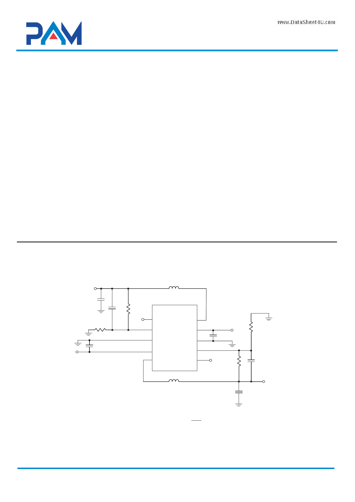
Typical Application
www.DataSheet4U.com
VOUT1
COUT1
10μF
R12
VIN2
CIN2
4.7μF
C Fw1
100nF
L1
R11 PAM2308
1
EN1
10
LX1
2
FB1
VIN1 8
4
GND
GND 9
3
VIN2
5 LX2
FB2 7
EN2 6
CIN1
4 .7 μF
VIN1
R21
R22
CFW2
100pF
L2
VOUT2
COUT2
10μF
( )VOUTx
=
VREF
1+
Rx1
Rx2
Figure 1. Adjustable Voltage Regulator
Power Analog Microelectronics,Inc
www.poweranalog.com
1
07/2008 Rev 1.0
1 page 
PAM2308
Dual High-Efficiency PWM Step-Down DC-DC Coverter
Electrical Characteristic
TA=25 OC, VIN=3.6V, VO=1.8V, CIN=10μF, CO=10μF, L=2.2μH, unless otherwise noted.
PARAMETER
Input Voltage Range
Regulated Feedback Voltage
Reference Voltage Line Regulation
Regulated Output Voltage Accuary
Peak Inductor Current
Output Voltage Line Regulation
Output Voltage Load Regulation
Quiescent Current (per channel)
Shutdown Current (per channel)
Oscillator Frequency
Drain-Source On-State Resistance
SW Leakage Current (per channel)
High Efficiency
EN Threshold High
EN Threshold Low
EN Leakage Current
Over Temperature Protection
SYMBOL
VIN
VFB
ΔVFB
VO
IPK
LNR
LDR
IQ
ISD
fOSC
RDS(ON)
ILSW
η
VEH
VEL
IEN
OTP
Test Conditions
IO = 100mA
VIN=3V,VFB = 0.5V or
VO=90%
VIN = 2.5V to 5V, IO=10mA
IO=1mA to 1A
No load
VEN = 0V
VO = 100%
VFB = 0V or VO = 0V
P MOSFET
IDS=100mA
N MOSFET
MIN TYP MAX
2.5 5.5
0.588 0.6 0.612
0.3
-3 +3
1.5
0.2 0.5
0.5 1.5
40 70
0.1 1
1.2 1.5 1.8
500
0.3 0.45
0.35 0.5
±0.01 1
96
1.5
0.3
±0.01
150
OTP Hysteresis
www.DataSheet4U.com
OTH
30
UNITS
V
V
%/V
%
A
%/V
%
μA
μA
MHz
kHz
Ω
Ω
μA
%
V
V
μA
°C
°C
Power Analog Microelectronics,Inc
www.poweranalog.com
5
07/2008 Rev 1.0
5 Page 
PAM2308
Dual High-Efficiency PWM Step-Down DC-DC Coverter
Application Information
The basic PAM2308 application circuit is shown
in Page 1. External component selection is
determined by the load requirement, selecting L
first and then Cin and Cout.
Inductor Selection
For most applications, the value of the inductor
will fall in the range of 1μH to 4.7μH. Its value is
chosen based on the desired ripple current.
Large value inductors lower ripple current and
small value inductors result in higher ripple
currents. Higher VIN or Vout also increases the
ripple current as shown in equation 1. A
reasonable starting point for setting ripple
current is △IL = 400mA (40% of 1A).
DIL
=
(f
1
)(L
)
VOUT
æ
çè
1-
VOUT
VIN
ö
÷ø
(1)
The DC current rating of the inductor should be
at least equal to the maximum load current plus
half the ripple current to prevent core saturation.
Thus, a 1.4A rated inductor should be enough for
most applications (1A + 400mA). For better
efficiency, choose a low DC-resis tance inductor.
Vo 1.2V 1.5V 1.8V 2.5V 3.3V
L 2.2μH 2.2μH 2.2μH 4.7μH 4.7μH
CIN and COUT Selection
www.DataSheet4U.com
In continuous mode, the source current of the top
MOSFET is a square wave of duty cycle
Vout/Vin. To prevent large voltage transients, a
low ESR input capacitor sized for the maximum
RMS current must be used. The maximum RMS
capacitor current is given by:
1
( )CIN required IRMS @ IOMAX éëVOUT VIN - VOUT ùû 2
VIN
This formula has a maximum at VIN =2Vout,
where IRMS=IOUT/2. This simple worst-case
condition is commonly used for design because
even significant deviations do not offer much
relief. Note that the capacitor manufacturer's
ripple current ratings are often based on 2000
hours of life. This makes it advisable to further
derate the capacitor, or choose a capacitor rated
at a higher temperature than required. Consult
the manufacturer if there is any question.
The selection of Cout is driven by the required
effective series resistance (ESR).
Typically, once the ESR requirement for Cout
has been met, the RMS current rating generally
far exceeds the IRI (PPLE P-P) requirement. The
output ripple △Vout is determined by:
VVOUT
@VIL
æçè ESR+
1
8fCOUT
ö
÷ø
Where f = operating frequency, COUT=output
capacitance and ΔIL = ripple current in the
inductor. For a fixed output voltage, the output
ripple is highest at maximum input voltage since
ΔIL increases with input voltage.
Using Ceramic Input and Output Capacitors
Higher values, lower cost ceramic capacitors are
now becoming available in smaller case sizes.
Their high ripple current, high voltage rating and
low ESR make them ideal for switching regulator
applications. Using ceramic capacitors can
achieve very low output ripple and small circuit
size.
When choosing the input and output ceramic
capacitors, choose the X5R or X7R dielectric
formulations. These dielectrics have the best
temperature and voltage characteristics of all
the ceramics for a given value and size.
Thermal consideration
Thermal protection limits power dissipation in
the PAM2308. When the junction temperature
exceeds 150°C, the OTP (Over Temperature
Protection) starts the thermal shutdown and
turns the pass transistor off. The pass transistor
resumes operation after the junction
temperature drops below 120°C.
For continuous operation, the junction
temperature should be maintained below 125°C.
The power dissipation is defined as:
( ) ( )PD =IO2
VORDSONH +
VIN -VO
VIN
RDSONL + tSWFSIO +IQ
VIN
IQ is the step-down converter quiescent current.
The term tsw is used to estimate the full load
step-down converter switching losses.
Power Analog Microelectronics,Inc
www.poweranalog.com
11
07/2008 Rev 1.0
11 Page | ||
| Páginas | Total 15 Páginas | |
| PDF Descargar | [ Datasheet PAM2308.PDF ] | |
Hoja de datos destacado
| Número de pieza | Descripción | Fabricantes |
| PAM2301 | 800mA Step-Down DC-DC Converters | Power Analog Micoelectronics |
| PAM2301 | 800mA STEP-DOWN DC-DC CONVERTER | Diodes |
| PAM2303 | 3A STEP-DOWN DC-DC CONVERTER | Diodes |
| PAM2304 | 1A STEP-DOWN DC-DC CONVERTER | Diodes |
| Número de pieza | Descripción | Fabricantes |
| SLA6805M | High Voltage 3 phase Motor Driver IC. |
Sanken |
| SDC1742 | 12- and 14-Bit Hybrid Synchro / Resolver-to-Digital Converters. |
Analog Devices |
|
DataSheet.es es una pagina web que funciona como un repositorio de manuales o hoja de datos de muchos de los productos más populares, |
| DataSheet.es | 2020 | Privacy Policy | Contacto | Buscar |