|
|
PDF AGR09085E Data sheet ( Hoja de datos )
| Número de pieza | AGR09085E | |
| Descripción | Lateral MOSFET | |
| Fabricantes | TriQuint Semiconductor | |
| Logotipo | ||
Hay una vista previa y un enlace de descarga de AGR09085E (archivo pdf) en la parte inferior de esta página. Total 8 Páginas | ||
|
No Preview Available !
AGR09085E
85 W, 865 MHz—895 MHz, N-Channel E-Mode, Lateral MOSFET
Introduction
The AGR09085E is a high-voltage, laterally diffused
metal oxide semiconductor (LDMOS) RF power tran-
sistor suitable for cellular band, code division multiple
access (CDMA), global system for mobile communi-
cation (GSM), enhanced data for global evolution
(EDGE), and time division multiple access (TDMA)
single and multicarrier class AB wireless base station
amplifier applications. This device is manufactured
on an advanced LDMOS technology offering state-
of-the-art performance, reliability, and best-in-class
thermal resistance. Packaged in an industry-stan-
dard package incorporating internal matching and
capable of delivering a minimum output power of
85 W, it is ideally suited for today's RF power ampli-
fier applications.
YLE 1
AGR09085EU (unflanged)
06, STYLE 1
AGR09085EF (flanged)
Figure 1. Available Packages
www.DataSheet4U.com
Features
Typical performance ratings are for IS-95 CDMA,
pilot, sync, paging, and traffic codes 8—13:
— Output power (POUT): 20 W.
— Power gain: 18 dB.
— Efficiency: 28%.
— Adjacent channel power ratio (ACPR) for
30 kHz bandwidth (BW):
(750 kHz offset: –45 dBc).
1.98 MHz offset: –60 dBc).
— Return loss: 10 dB.
High-reliability, gold-metalization process.
Best-in-class thermal resistance.
Internally matched.
High gain, efficiency, and linearity.
Integrated ESD protection.
Si LDMOS.
Industry-standard packages.
85 W minimum output power.
Table 1. Thermal Characteristics
Parameter
Thermal Resistance,
Junction to Case:
AGR09085EU
AGR09085EF
Sym
R JC
Value
0.7
0.7
Unit
°C/W
Table 2. Absolute Maximum Ratings*
Parameter
Sym Value Unit
Drain-source Voltage
VDSS 65 Vdc
Gate-source Voltage
VGS –0.5, 15 Vdc
Drain Current—Continuous ID 8.5 Adc
Total Dissipation at TC = 25 °C:
AGR09085EU
PD 250 W
AGR09085EF
250
Derate Above 25 C:
AGR09085EU
1.43 W/°C
AGR09085EF
1.43
Operating Junction Tempera- TJ 200 °C
ture
Storage Temperature Range TSTG –65, 150 °C
* Stresses in excess of the absolute maximum ratings can cause
permanent damage to the device. These are absolute stress rat-
ings only. Functional operation of the device is not implied at
these or any other conditions in excess of those given in the
operational sections of the data sheet. Exposure to absolute
maximum ratings for extended periods can adversely affect
device reliability.
Table 3. ESD Rating*
AGR09085E
HBM
MM
CDM
Minimum (V)
500
50
1500
Class
1B
A
4
* Although electrostatic discharge (ESD) protection circuitry has
been designed into this device, proper precautions must be
taken to avoid exposure to ESD and electrical overstress (EOS)
during all handling, assembly, and test operations. PAEgeArKe Devices
employs a human-body model (HBM), a machine model (MM),
and a charged-device model (CDM) qualification requirement in
order to determine ESD-susceptibility limits and protection
design evaluation. ESD voltage thresholds are dependent on the
circuit parameters used in each of the models, as defined by
JEDEC's JESD22-A114B (HBM), JESD22-A115A (MM), and
JESD22-C101A (CDM) standards.
Caution: MOS devices are susceptible to damage from elec-
trostatic charge. Reasonable precautions in han-
dling and packaging MOS devices should be
observed.
1 page 
AGR09085E
85 W, 865 MHz—895 MHz, N-Channel E-Mode, Lateral MOSFET
Typical Performance Characteristics (continued)
0
-10
-20
-30
ACP+
-40
-50
-60
-70
0.00
ALT1+
ACP-
ALT-
5.00 10.00 15.00 20.00 25.00 30.00 35.00
POUT (W)S
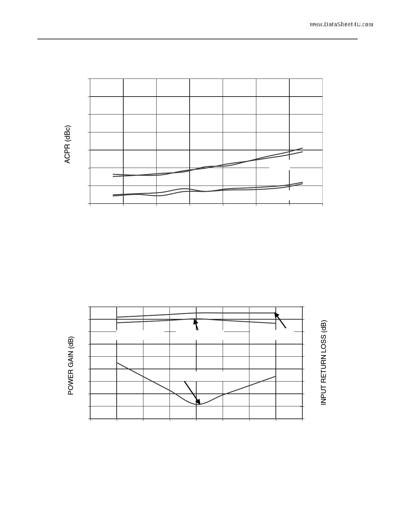
TEST CONDITIONS:
VDD = 28 Vdc, IDQ = 0.8 A, TC = 30 °C.
FREQUENCY = 880 MHz; IS-95 CDMA PILOT, PAGING, SYNC, TRAFFIC CODES 8 THROUGH 13; OFFSET 1 = 750 kHz;
OFFSET 2 = 1.98 MHz; OFFSET 1 AND 2 BW = 30 kHz.
Figure 4. ACPR vs. POUT
19
www.DataSheet4U.com
18
17 POWER GAIN POUT = 100 W
16
15
14
13 RETURN LOSS
12
11
10
860 865 870 875 880 885
FREQUENCY (MHz)A
TEST CONDITIONS:
VDD = 28 Vdc, IDQ = 0.8 A, TC = 30 °C, WAVEFORM = CW.
0
-2
POUT = 10 W
-4
-6
-8
-10
-12
-14
-16
-18
890 895 900
Figure 5. Power Gain and Return Loss vs. Frequency
5 Page | ||
| Páginas | Total 8 Páginas | |
| PDF Descargar | [ Datasheet AGR09085E.PDF ] | |
Hoja de datos destacado
| Número de pieza | Descripción | Fabricantes |
| AGR09085E | Lateral MOSFET | TriQuint Semiconductor |
| Número de pieza | Descripción | Fabricantes |
| SLA6805M | High Voltage 3 phase Motor Driver IC. |
Sanken |
| SDC1742 | 12- and 14-Bit Hybrid Synchro / Resolver-to-Digital Converters. |
Analog Devices |
|
DataSheet.es es una pagina web que funciona como un repositorio de manuales o hoja de datos de muchos de los productos más populares, |
| DataSheet.es | 2020 | Privacy Policy | Contacto | Buscar |
